TTL Circuits:
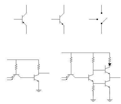
BJT may realize the switch illustrated in Figure (c) as we have discussed above.
The most basic TTL logic gate is NAND gate as illustrated in Figure (d). In this circuit, TA is a multiple emitter transistor and in this transistor there is only one collector and base but there are multiple emitters. Here the multiple base emitter junction acts just like independent diodes. The real practical circuit has an additional totem pole output driver as illustrated in Figure (e). Let us try to understand how this circuit acts like a NAND gate. When Input1 and Input2 are at 0 V, the multiple emitter base junctions of transistor TA are forward biased while the base collector is reverse biased and transistor TB remains off and thus the output voltage is equal to Vcc. As the base voltage for transistor TC is Vcc, this transistor is on and the output is also Vcc. And the input to transistor TD is 0 V, therefore it remains off. When one of the Input 1 and Input 2 is 0 V, the corresponding collector emitter junction of transistor TA is conducting then it has the same operation with the previous case and the output is at Vcc. For the case when Input1 and Input 2 are at Vcc, both the base emitter junctions are reverse biased and the base collector junction of the transistor TA is forward biased so the transistor TB is on. Thus the input to transistor TC is 0 V and the input to transistor TD is 0.8 V therefore TD is on. Thus the output voltage at the collector of transistor TB is 0.8 V + VCES (saturation voltage among conductor and emitter of a transitor is equal to 0.2 V) = 1 V. Since Diode D is present TC remains in off state. But TD is on, the collector emitter voltage of the TD in saturation is 0.2 V and the output is also equal to 0.2 V, that means at logic 0.

Figure: (a) npn BJT, (b) pnp BJT, (c) Switch Configuration, (d) Simplified TTL NAND Gate, and (e) TTL NAND Gate with Totem Pole Output Configuration