Digital Inverter:
Inverter carry out the function of logic negation or output voltage V0 is the inverse or complement of the input voltage Vi or it is also termed as NOT logic gate.
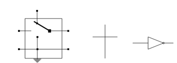
Figure (a) depicts the switch configuration for realization of a Digital Inverter. Whereas input is low, the switch is connected to Vcc, and the output is high. Whereas the input is high, the switch is connected to the ground and the output is low as list in the form a truth table as shown in Figure (b). The symbol for Digital Inverter is drawn in Figure (c).

(a) (b) (c)
Figure: (a) Switch Configuration, (b) Truth Table, and (c) Symbol of a Digital Inverter