Digital Buffer:
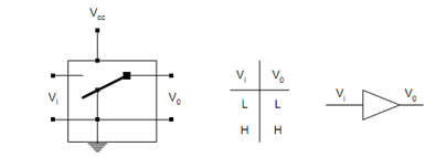
A buffer may be realized by using a switch as depicted in Figure (a), which is operated by the input voltage Vi. Whereas Vi is low, the switch is connected to ground and output voltage V0 is low. Whereas Vi is high, the switch is connected to Vcc and the output voltage V0 is high. It may be tabulated in the form of a truth table as illustrated in Figure (b), where the output follows the value of the input. Figure (c) illustrates the symbol of a Digital Buffer.

(a) (b) (c)
Figure: (a) Switch Configuration, (b) Truth Table, and (c) Symbol of a Digital Buffer