Small Signal Equivalent Model:
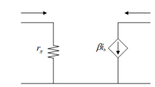
The small signal model for the common emitter transistor is drawn in Figure. Here we have replaced the diode with a linear element (a resistor, called rπ) and we have utilized the notation for the currents ib and ic since now we are considering small signal ac quantities, not high signal ones. This model is only utilized to figure out how the transistor behaves for the ac signal going through it, not how it responds to high dc values.

Figure: Small Signal Linear Model for the Common Emitter Transistor
Now rπ the equivalent small signal resistance of the base-emitter diode is simply given by the inverse of the conductance of the equivalent diode.
rπ = β /40 IC
The typical values for β in a standard bipolar transistor shall be around 100. Therefore, for a typical collector bias current of IC = 1 mA, rπ shall be about 2.5 k?. Remember, we said that the current coming out of the collector is not affected by how big the drop was in the reverse biased base-collector junction. The collector current just based on how many electrons are injected into the base by the emitter, and how several make it across the base to the base-collector junction. As enhancing VCE increase the base-collector reverse bias, the depletion width of the base-collector junction increase as well. It has the effect of making the base region somewhat shorter. It means that a few more electrons are able to make it across the base region without recombining and consequently α and therefore β increases. That means that IC goes up slightly with enhancing VCE. The effect is called base width modulation. Now Let us include that effect in the common emitter characteristic curves. As you may see in Figure, IC enhancing somewhat as VCE increases. The effect has been somewhat exaggerated in Figure, and I shall now make the slope even bigger so that we can define a new quantity, called the Early Voltage.

Figure: Common Emitter Response with Base-width Modulation Effect and Early Voltage