MOSFET:
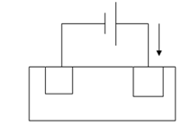
We shall now focus on a device called the Metal-Oxide-Semiconductor Field Effect Transistor or just, the MOSFET. Consider the following:

Figure: How Does Field Effect Transistor Comes into Picture?
Here we have a block of silicon, doped p-type. Into it we have built two regions, which are doped n-type. These n-type regions are linked to a battery. If we try to get some current, I, to pass through this structure, nothing shall happen; because the n-p junction on the RHS is reverse biased (We have the positive lead from the battery going to the n-side of the p-n junction.) If we effort to remedy this by turning the battery around, now we shall have the LHS junction reverse biased, and again, no current shall flow. If, for whatever reason, we want the current to flow, we shall need to come up with some of the way of forming a layer of n-type material among one n-region and the other. This shall then connect them together, and we may run current in one terminal and out the other. To see how we shall do this, let's do two things. First we shall grow a layer of SiO2 (silicon dioxide) over the silicon. (it turns out to be relatively easy; we just stick the wafer in an oven with some oxygen flowing through it, and heat everything up to about 1100°C for an hour or so, and we end up with high-quality insulating SiO2 layer over the silicon.) Over the oxide layer then we deposit a conductor, which we call the gate. In the olden days, the gate would have been a layer of aluminum (therefore, the name metal-oxide-silicon or MOS). Nowadays, it is much more likely that a heavily doped layer of polycrystalline silicon (polysilicon) would be deposited to form the gate structure.