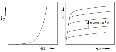
Transfer and Output Characteristics:
The transfer characteristics are plot of the collector current iC as a function of the
base-to-emitter voltage vBE along the collector-to-emitter voltage vCE held constant. From
iS and ic equations we can write
iC = I SO (1 + (υCE / VA )) exp (υ BE / VT )
It follows that iC varies exponentially with vBE ,the plot of which is given in Figure It may be seen from the plot that the collector current is nesessary zero until the base-to-emitter voltage reaches a threshold value. Above this particular value, the collector current enhanced rapidly. The threshold value is typically in the range of 0.5 to 0.6 V. For high current transistors, usually it is smaller. The plot illustrates a single curve. If vCE is enhanced, the current for a given vBE is larger. Though, the displacement between the curves is so small that it may be difficult to distinguish between them. The small-signal transconductance gm is described as the slope of the transfer characteristics curve evaluated at the quiescent or dc operating point for a device.

Figure: BJT Transfer and Output Characteristics
The output characteristics are a plot of the collector current iC as a function of the collector-to-emitter voltage vCE with the base current iB held constant. Through ic and β eq we may write
iC = β0 (1 + (υ CE /VA) iB
It follows that iC varies linearly with vCE. A plot of this variation is given in Figure. For small vCE such 0 ≤ vCE < vBE, Eq. (9) does not hold. In the region in Figure where this holds, the BJT is saturated. The small-signal collector-to-emitter resistance ro is described as the reciprocal of the slope of the output characteristics curve evaluated at the quiescent or dc operating point for the device.