Hybrid-π Model of a Transistor:
Let each voltage and current be written as the sum of a dc component and a small-signal ac component as follows :
iC = IC + ic iB = I B + ib
vBE = VBE + vbe vCE = VCE + vce
If the ac components are adequately small, we can write
ic = (∂IC /∂VBE ) vbe + ∂IC/∂Vce ; ib = ∂IB/∂VBE vbe
where the derivatives are evaluated at the dc bias values. Three useful small signal parameters of the BJT, known as its trans-conductance gm, the collector-to-emitter
resistance r0, and the base-to-emitter resistance rπ, can be defined now as follows :
gm = ∂IC / ∂VBE = IS /VT exp(VBE /VT ) = IC /VT
ro = (∂I/ ∂ VCE )-1 = [(ISO /VA )exp (VBE /VT)]-1 = (VA+VCE/IC)
r π = ( ∂I B /∂VBE ) -1 = [ (ISO / β0 VT ) exp (VBE/ VT)]-1 = VT/IB
The collector and base currents can, thus, be written as
i c = i′c + (v ce /r0 ); i = vπ / rπ
where
ic′ = gm vπ ; vπ = vbe
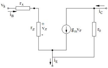
The small-signal circuit which models these equations is specified in Figure. It is called the hybrid-π model. The resistor rx, which does not show in the above equations, is known as the base spreading resistance. It show the resistance of the connection to the base region inside the device. Since the base region is extremely narrow, the connection exhibits a resistance which frequently cannot be neglected.

Figure: Hybrid π Model
The small-signal base-to-collector ac current gain β is described as the ratio ic′ / ib. It is given by
β= ic′ /ib = gm vπ /ib = gm rπ = (IC /VT )( VT / IB) = IC / IB
Note that ic differs from i′c by the current through r0. Therefore, ic/ ib ≠ β , unless r0 = ∞.