Bipolar Junction Transistor:
The notations utilized here for voltages and currents correspond to the following conventions : DC bias values are mentioned by an upper case letter with upper case subscripts, for example IC , VDS. Instantaneous values of small-signal variables are mentioned by a lower-case letter with lower-case subscripts, e.g. υs, ic. Total values are indicated by a lower-case letter with upper-case subscripts, foe instance. υBE, iD. Circuit symbols for independent source are circular and symbols for controlled sources have a diamond shape. Voltage sources have a ± sign within the symbol and current sources have an arrow.
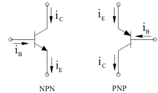
Figure illustrated the circuit symbols for the NPN and PNP BJTs. The collector-base junction is reverse-biased and the base-emitter junction is forward biased in the active mode. For the NPN device, the active-mode collector and base currents are specified by
iC = I S exp(υ BE /VT) ; iB = iC / β

Figure: BJT Circuit Symbols
where VT refer to the thermal voltage, IS refer to the saturation current, and β is refers to the current gain. These are given by
VT = kT/ q = 0.025 V for T = 290; K = 25.86 m V for T = 300 K
IS = ISO (υCE /VA)
and
β= β0 (1 + (υCE /VA ))
where VA is the early voltage and ISO and βo, respectively, are the zero values of IS and β.
Because I S/ β = ISO/ β0 , it follows that i is not a function of υCE. The equations apply to the pnp device if the subscripts BE and CE are reversed.
The emitter-to-collector current gain α is defined as the ratio iC / iE .To solve for this, we
may write
i E = i B + i C = ((1/ β )+ 1) i C = (1 + β/ β) i C
It follows that
α= iC/ iE = β/1 + β
Therefore, the three transistor currents are associated by the equation
iC =β iB = α iE