Depletion Versus Enhancement:
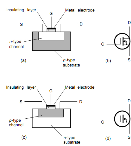
In JFET, the channel conducts with zero bias, that is, whenever the potential difference among the gate and the source is zero. Since the depletion area grows, the charge carriers pass via a narrowed channel. It is termed as depletion mode. The MOSFET can work in depletion mode, too. The schematic symbols and drawings of the figure shown below represent depletion-mode MOSFETs.

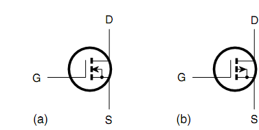
Metal-oxide-semiconductor method permits a second mode of operation. The enhancement-mode MOSFET has a pinched-off channel at zero bias. It is essential to apply a gate bias voltage EG to build a channel. When EG = 0, then the drain current ID is also zero whenever there is no signal input. The schematic symbols for n-channel & p-channel enhancement-mode devices are shown in figure below. In schematic diagrams, they can be distinguished from depletion-mode devices by looking at the vertical lines within the circles. Depletion mode MOSFETs contains solid vertical lines; enhancement-mode devices consist of broken vertical lines.

Figure: (a) The symbol for an n-channel enhancement-mode MOSFET. (b) The sign for a p-channel enhancement-mode MOSFET.