Behavior of a P-N junction:
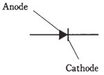
Simply having a semiconducting material, may be P or N type, this might be interesting, and a good object of science experiments. But when 2 types of material are brought together, P-N junction develops properties which make the semiconductor materials truly useful as the electronic devices. Figure B which is given below shows the schematic symbol for the semiconductor diode, formed by joining the piece of P-type material to the piece of N-type material. The N-type semiconductor can be represented by the short, straight line in symbol, and is called as cathode. The P-type semiconductor can be represented by the arrow, and is termed as anode.
In diode as shown in the figure, electrons flow in direction opposite arrow. But current cannot, flow the other way under most conditions. Electrons normally do not flow in direction in which the arrow points. If you connect the battery and the resistor in series with diode, you will get a current flow if negative terminal of battery is connected to cathode and positive

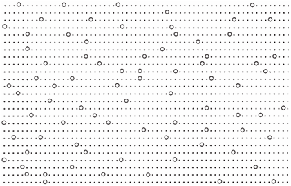
Figure-- Pictorial representation of hole flow. Small dots represent electrons, moving in one way; open circles represent holes, moving in the other way.

Figure-- Schematic symbol for a semiconductor diode.
terminal is connected to anode. No current will flow if battery is reversed. The resistor is included in circuit to prevent destruction of diode by the excessive current.
It takes a certain minimum voltage for conduction to take place. This is called as forward breaker voltage of junction. Depending on type of material, it ranges from about 0.3 V to 1 V. If voltage across the junction is not at least as great as forward breaker value, diode will not conduct. This effect can be of use in the waveform clippers, amplitude limiters, and threshold detectors.