IGBT:
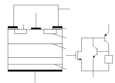
The Insulated Gate Bipolar Transistor or IGBT for short combines the high dc current gain of a MOSFET with the high current handling capability and high blocking voltage of a BJT in a surprisingly simple structure such as the one illustrated in Figure. At first glance, the vertical structure looks like that of a regular bipolar transistor structure. However a closer look reveals a p+ substrate instead of an n+ substrate. Its operating principle combines those of MOSFET, the bipolar transistor and power diode. To further analyze this structure we use the equivalent circuit, which contains the pnp BJT as composed by the bottom three layers as well as the nMOSFET underneath the gate electrode. One must note down that the p-type collector of the pnp BJT and the n-type source of the nMOSFET share the similar metal contact. Also, that drain region of the nMOSFET is the buried n-type layer that is the n-type base of the pnp BJT. The electrons originating from the n+ source flow laterally underneath the gate and then flow down in the buried n-type region, thus supplying the gate current of the pnp BJT.
As the gate current is provided locally, the emitter current shall be concentrated around the same area. Note down that under typical operation the collector would be grounded whereas the positive voltage is applied to the emitter. Thus this device can be connected in a switching circuit just like an npn BJT with the significant distinction that no gate current is required to maintain the on-state current.

(a) (b)
Figure: (a) IGBT Structure; and (b) Equivalent Circuit