Half-Wave Voltage Doublers
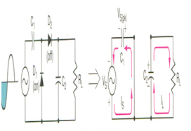
The operation of the half- wave doubler is simpler to understand if we suppose that the diodes are ideal components. At the time of the negative alternation of the input as indicate in the diagram, D1 is forward - biased & D2 is reverse-biased by the input signal polarity. If we show D1 like a short circuit & D2 like open, we obtain the equivalent shown in the diagram. Since you can see the, C1 shall charge till its plat-to-plate voltage is equivalent to the source voltage. At the similar time , C2 shall be in the procedure of discharging through the load resistance RL.

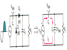
While the input polarity reverses, we contain the circuit conditions indicate in the diagram below. As D1 is off, this is represented like an open in the correspondent circuit. Also , D2 (which is on ) is shown as a short. By using the correspondent circuit, this is easy to see that C1(that is charged to the peak value of Vs) and now the source voltage behave as series -aiding voltage sources. Therefore, C2 shall charge to the total of the series peak voltages.2VS(pk) .

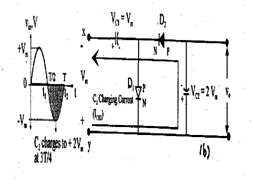
- Throughout the first half cycle pt x is positive with respect to pt y of the input. A charging current shall be forced via capacitor C1 and diode D1 that shall be forward biased.
- Capacitor C1 shall charge to the peak for the time T/4. Throughout the same time D2 shall remain off.

Throughout the negative half cycle of the input point x shall be negative with respect to y & voltage of C1 (Vc1 & Vin) are in additive or series.
A current shall try to follow from y to x but D1 does not permit as it is off. But D2 shall be conducting.
This lets C2 to charge up because of the current Ich2 shall follows from point y by C2 by D2 & back to point x. Voltage on C2 shall be of magnitude 2Vm.
By applying KVL we can say
-Vc1 - Vin = Vo
however
Vc1 = Vmax
therefore
V0 = -2V
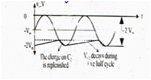
Output waveform shall be as
