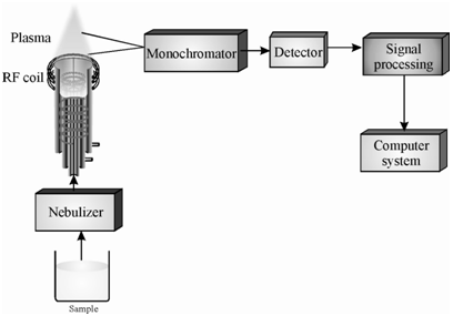
Schematic layout of different components:
A schematic layout of an ICP-AES spectrometer is given in Figure. The sample in the solution form is nebulised and injected into the plasma source with the help of a suitable nebuliser. The emitted radiation is passed by monochromator and after dispersion it is detected by a photodetector and sent to the processing unit for the processing and generating suitable output.

Figure: A schematic layout of different components of an ICP-AES spectrometer
You have learnt about the creation and features of various kinds of plasma source in the previous section. While we are discussing about the instrumentation for ICP-AES, the inductively coupled plasma acts as a source.