T-type Flip Flops:
Let us learn clocked pulse first. It shall be a little bit of digression, but this shall be necessary to understand Toggle Flip Flop properly. To bring synchronism into digital circuits numerous digital systems are clocked or pulsed and they operate in synchronism with a pulse train of period T shown in Figure. The pulse width tp is supposed small compared to the time period T. The binary values are supposed to be constant during any interval T and it changes its state throughout clocked pulse either at the negative transition (negative triggered Flip Flops) or positive transition (positive triggered Flip Flops) of the pulse. Any output value of the logic circuit at the nth time instant (nT time interval) is represented by Qn and at (n + 1)th time instant ((n + 1) T time interval) is depicted by Qn + 1.

Figure: Clock Pulse Train to Synchronize Sequential Digital Circuits
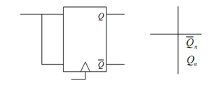
The T-type Flip Flop modifies its states with every clocked pulse and therefore it is called as Toggle (T) Flip Flop. T Flip Flops are realized by shorting the two input terminals of a JK Flip Flop as illustrated in Figure 8.25(a) and its truth table is drawn in Figure 8.25(b). Let us try to understand the truth table for such Flip Flops. When T = J = K = 1, Q toggles between 0 and 1 as the clock makes transition and hence it gives increase to toggling. Generally the T input is tied to 1 to make this happen. While T = 0, it behaves as a D type Flip Flop. It must be noted that we may not construct T-type Flip Flops from SR Flip Flops since S = R = 1 is forbidden for SR Flip Flops.

(a) (b)
Figure: (a) Toggle Flip Flop, and (b) Truth Table of T Flip Flop