Voltage amplification
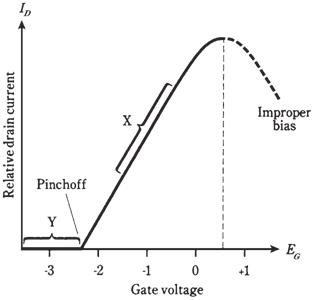
The graph given in the figure given below shows the drain current, ID, as a function of gate bias voltage, EG, for a hypothetical N-channel JFET. The drain voltage, ED, is supposed to be constant.

Figure-- Relative drain current as a function of gate voltage for a hypothetical N-channel JFET
When EG is large and negative, the JFET is pinched off, and no current flows through channel. As EG becomes less negative, the channel opens up, and current starts flowing. As EG becomes still less negative, the channel gets broader and the current ID increases. As EG approaches point where SG junction is at forward breakover, the channel conducts as well as it possibly can.
If EG becomes positive sufficiently so that the SG junction conducts, the JFET will not work properly. Some of the current in channel will then be shunted off through gate, a situation which is never desired in a JFET.The best amplification for weak signals can be obtained when gate bias, EG, is such that slope of curve in the figure given below is the greatest. This is shown by the range marked X in figure. For power amplification, results are often best when the JFET is biased at, or even beyond it, pinchoff, in range marked Y.
The current ID passes through drain resistor, as shown in diagram of Figure given below. Small fluctuations in EG cause large changes in ID, and these variations in turn produce wide swings in the direct current voltage across R3 or R4. The alternating current part of this voltage goes through the capacitor C2, and appears at output as a signal of much greater alternating current voltage than that of input signal at the gate. That is voltage amplification.