Super-high input impedance
When MOSFET was 1st developed, it was known an insulated-gate FET or IGFET. This is more descriptive of the device than currently accepted name. The gate electrode is insulated actually, by a thin layer of dielectric, from channel. As a result, the input impedance is higher than that of a JFET; the gate to source resistance of the typical MOSFET is comparable to that of the capacitor! This means that a MOSFET draws essentially no current, and thus no power, from the signal source. Some MOSFETs have input resistance which is exceeding a trillion (1012) ohms.
The main problem
The trouble with the MOSFETs is that they can be damaged easily by static electric discharges. When building circuits containing MOS devices, technicians should use special equipment to ensure their hands do not carry static charges which might ruin the components. If the static discharge occurs through dielectric of a MOS device, the component will be permanently destroyed. Warm and humid climates do not give protection against hazard.
Flexibility
In the actual circuits, an N-channel JFET can at times be replaced directly with the N-channel MOSFET; P-channel devices can be interchanged similarly. But the characteristic curves for the MOSFETs are not same as those for JFETs. The basic difference is that SG junction in a MOSFET is not a P-N junction. Thus, forward breakover cannot take place. An EG of over 0.6 V can be applied to an N-channel MOSFET, or an EG negative than 0.6 V to a P-channel device, without current leak taking place.
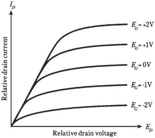
A family of characteristic curves for the hypothetical N-channel MOSFET is shown in graph given below. The device will work with the positive gate bias as well as with the negative gate bias. A P-channel MOSFET behaves in the similar fashion, being usable with positive or negative EG.

Figure-A family of characteristic curves for a hypothetical N-channel MOSFET