JFET biasing
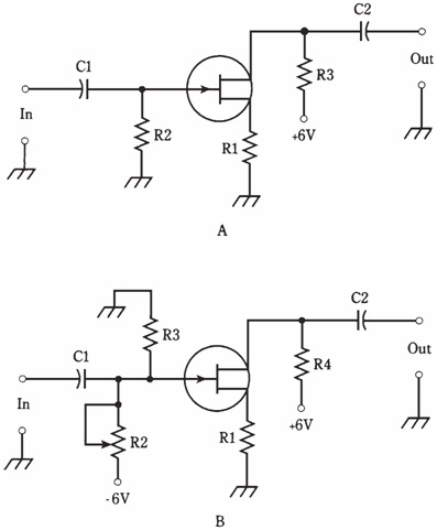
Two biasing arrangements for an N-channel JFET are shown in the figure given below. These hookups are similar to the manner an NPN bipolar transistor is connected, except that source-gate (SG) junction is not forward-biased.
At point A, the gate is grounded through the resistor R2. The source resistor, R1, limits current through JFET. The drain current, ID, flows through R3, generating a voltage across this resistor. The alternating current output signal passes through C2.
At point B, the gate is connected to a voltage that is negative with respect to ground through potentiometer R2. By adjusting this potentiometer results in variable negative EG between R2 and R3. Resistor R1 restricts the current through JFET. The drain current, ID, flows through R4, generating a voltage across it; the alternating current output signal passes through C2.
In both of the circuits, the drain is positive relative to ground. For the P-channel JFET, reverse the polarities as in the Figure given below. The connections are similar to the way a PNP bipolar transistor is used, except SG junction is not forward-biased.

Figure--Two methods of biasing an N-channel JFET. At point A, fixed gate bias; at Point B, variable gate bias.
Typical JFET power supply voltages are comparable to those with the bipolar transistors. The voltage between source and drain, abbreviated ED, can range from around 3 V to 150 V; often it is 6 V to 12 V.The biasing arrangement in the given is commonly used for weak-signal amplifiers, oscillators and low-level amplifiers. The scheme at point B is more often employed in the power amplifiers having the substantial input signal.