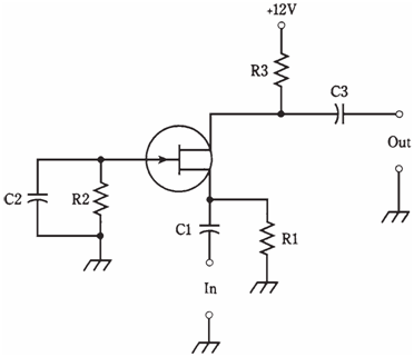
Common-gate circuit
The common-gate circuit has the gate at signal ground. The input is applied to source. The illustration shows an N-channel JFET, for other types of FETs, same considerations apply as described above for common-source circuit. Enhancement-mode devices would need a resistor between gate and positive supply terminal (or negative terminal if MOSFET is P-channel).

Figure-Common-gate circuit configuration
The direct current bias for the common-gate circuit is basically same as that for the common-source arrangement. But signal follows a different path. The alternating current input signal enters through C1. Resistor R1 keeps input from being shorted to ground. Gate bias is given by R1 and R2; capacitor C2 places gate at signal ground. In some common gate circuits, the gate electrode is grounded directly, and components resistor R2 and capacitor C2 are not used. The output leaves the circuit through the capacitor C3. Resistor R3 keeps the output signal from being shorted through the power supply.
The common-gate arrangement generates less gain than the common source counterpart. But this is not bad at all; a common gate amplifier is stable, and is not likely to break into unwanted oscillation. The output is in phase with input.