Differential Mode and Common Mode Gains:
The voltages V01 and V02 are given by
V01.2 = VCC - IC1, 2 RC
where we suppose RC1 = RC2 = RC. Plots of V01 and V02 versus VD may be made similar to those of Figure In the range - 2 ≤ VD /VT ≤ + 2, VOD change almost linearity with VD.
Therefore, in this range the circuit acts as a linear differential amplifier.
To get an analytical expression for VOD in terms of VD, we write
VOD = V01 - V02
= (IC 2 - IC1 ) RC [from Eq. (43)]
= I EE RC [ (1 + e -VD /VT ) -1 - (1+1 + e+ (VD /VT ) ) -1 ] - [From Eqs. (41) and 42)]
The above may be written as :
V OD ≅- I EE R C tanh [ VD/(2VT )]
obviously, for VD < - 2 VT, V0 ≅ - I EE RC and for VD > 2 VT ,
V = (I EE RC /2V T )V D
If the sources are taken as vs1 = vs/2 and vs2 = - vs/2 so that the differential input signal is
vd = vs1 - vs2. This results in small signal base voltages that are equal and opposite, and
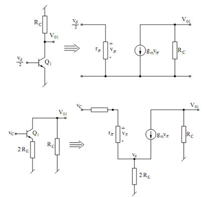
Due to symmetry, it follows that the ac current through REE must be zero. This, in turn, means ve = 0; in other terms, the common emitter node may be taken as ac ground. The total circuit thus simplifies to that illustrated in Figure, which is called the differential mode half circuit. That its output voltage is vod/2 must be obvious from symmetry. From this circuit, the reader may easily find that
Ad = vod /vd = (vod/ 2) / (vd/2) = - gm Rc

Figure: Equivalent Circuits for the Calculation of Differential Mode and Common Mode Gains