NPN AND PNP:
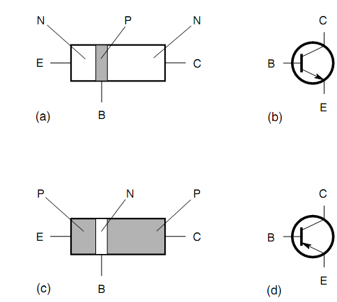
The simplified drawing of an npn transistor and the symbol which is used to symbolize it in schematic diagrams are shown in figure below. The p-type, or center, layer is the base. Thinner of the n-type semiconductors is the emitter, and the thicker is the collector. At times these are labeled B, E, & C in schematic diagrams, though the transistor symbol points out which is which (the arrow is at the emitter). A pnp transistor (parts c & d) has two p-type layers, one on any side of a thin n-type layer. In the npn sign, the arrow points outward. In the pnp sign, the arrow points inward.
Normally, pnp and npn transistors can perform the same tasks. The only difference is the polarities of the voltages and the directions of the currents. In most of the applications, an npn device can be substituted with a pnp device, or vice-versa, and the power-supply polarity oppose, and the circuit will still work when the new device has the suitable specifications.
There are various types of bipolar transistors. A few are used for rf amplifiers and oscillators; others are intended for audio-frequencies (af). Some can handle high power for rf wireless transmission or af hi-fi amplification, and others are made for the weak-signal rf reception, microphone pre-amplifiers, & transducer amplifiers. Some are produced for switching, and others are planned for signal processing.

Figure: Pictorial diagram of npn transistor (a), schematic symbol for npn transistor (b), pictorial diagram of pnp transistor (c), and schematic symbol for pnp transistor (d).