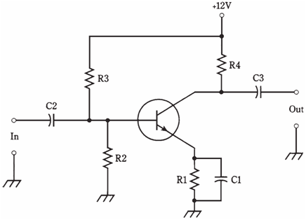
Common emitter circuit:
A transistor can be hooked up in 3 general ways. The emitter can be grounded for the signal, base can be grounded for signal, or collector can be grounded for the signal. Probably the mostly used arrangement is common-emitter circuit. Common means grounded for signal. The basic configuration is given in the figure below.
A terminal can be at ground potential for signal, and yet have a significant direct current voltage. In circuit shown, C1 looks like a dead short to the alternating current signal, so emitter is at signal ground. But R1 causes emitter to have a certain positive direct current voltage with respect to ground (or negative voltage, if PNP transistor is used). The exact direct current voltage at emitter depends on value of R1, and on the bias.

Figure-- Common-emitter circuit configuration.
The bias is set by ratio of resistances R2 and R3. It can be vary from zero, to ground potential, to + 12 V, the supply voltage. Usually it will be a couple of volts. Capacitors C2 and C3 block direct current to or from input and output circuitry (whatever that may be) while letting the alternating current signal pass. Resistor R4 keeps the output signal from being shorted out through power supply.
A signal voltage enters common emitter circuit through C2, where it makes the base current, IB to vary. The fluctuations in IB make large changes in the collector current, IC. This current passes from R4, causing a fluctuating direct current voltage to appear across this resistor. The alternating current part of this passes unhindered through C3 to output.
The circuit of it which is given in the figure is the basis for many amplifiers, from audio frequencies through the ultra high radio frequencies. The common emitter configuration generates largest gain of any arrangement. The output is 180 °out of phase with the input.