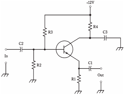
Common-collector circuit:
A common-collector circuit shown in the figure given below operates with the collector at signal ground. The input is applied at base just as it is with common-emitter circuit.
The signal passes through C2 onto base of transistor. Resistors R2 and R3 gives the correct bias for base. Resistor R4 limits current through the transistor. Capacitor C3 keeps collector at signal ground. A fluctuating direct current flows from R1, and a fluctuating direct current voltage thus appears across it. The alternating current part of this voltage passes through C1 to output. Because the output follows emitter current, this circuit is called as emitter follower circuit.

Figure--Common-collector circuit configuration. This arrangement is known as an emitter follower.
The output of this circuit is in phase with input. The input impedance is very high, and the output impedance is low. For this very reason, the common collector circuit can be used to match high impedances to low impedances. When a designed, an emitter follower works over the extensive range of frequencies, and is a low cost alternative to the broad band impedance matching transformer.