Zero-bias equilibrium, Electrical Engineering

Assignment Help:

Zero-Bias Equilibrium

In a p-n junction, with no an external applied voltage, an equilibrium condition is arrived at in which a potential variation is formed across the junction. This potential difference is termed as built-in potential Vbi.

Later than joining p-type and n-type semiconductors, electrons that are near the p-n interface tend to diffuse into the p region. As electrons diffuse, they depart positively charged ions (donors) in the n region. Likewise, holes near the p-n interface start to diffuse into the n-type region leaving fixed ions (acceptors) along with negative charge. The regions near the p-n interfaces lose their neutrality and become charged, creating the space charge region or depletion layer.

616_Zero-Bias Equilibrium 1.png

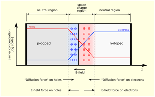
Figure: A p-n junction in thermal equilibrium with zero bias voltage applied. Electrons and holes concentration are reported correspondingly with blue and red colored lines. Gray regions are charge neutral. Light red zone is charged positively. Light blue zone is charged negatively. The electric field is displayed on the bottom, the electrostatic force on electrons and holes and the direction in which the diffusion tends to move electrons and holes.

The electric field that is created by the space charge region opposes the diffusion procedure for both electrons and holes. There are 2 concurrent phenomena: the diffusion process which tends to produce more space charge and the electric field produced by the space charge which tends to counteract the diffusaion. The carrier concentration profile at equilibrium is displayed in figure with blue and red colored lines. As well shown are the two counterbalancing phenomena which establish equilibrium.

1054_Zero-Bias Equilibrium 2.png

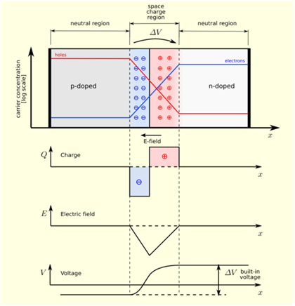
Figure:  A p-n junction in thermal equilibrium with zero bias voltage applied. Within the junction, plots for the charge density, the electric field and the voltage are reported.

The space charge region is a zone with a net charge that is provided by the fixed ions (donors or acceptors) which have been left uncovered via majority carrier diffusion. While equilibrium is arrived at, the charge density is approximated through the displayed step function. Actually, the region is totally depleted of majority carriers (leaving a charge density equal to the net doping level), and the edge among the space charge region and the neutral region is quite sharp. The space charge region has similar charge on both sides of the p-n interfaces, so it extends farther on the less doped side.


Related Discussions:- Zero-bias equilibrium

Explain thermosetting plastic materials, Explain Thermosetting Plastic Ma...

Explain Thermosetting Plastic Materials. Thermosetting Plastic Materials: They undergo huge changes while subjected to high temperatures for rather sometimes. They are call

Each cells is connected 4 rows, 20 cells with emf 1.45V and internal resist...

20 cells with emf 1.45V and internal resistance 0.5Ω for each cells is linked 4 rows which every rows having of 5 cells in series. Load resistance 15Ω is connected to the battery.

Error in simulink, dear sir, when i am going to simulate my model in matlab...

dear sir, when i am going to simulate my model in matlab i am getting the following error : the derived input for the integrator is inf or nan at time xxxxx. try to reduce the step

Decimal to binary coded decimal conversions, Decimal to Binary Coded Decima...

Decimal to Binary Coded Decimal Conversions Step1. Separate the digits in the decimal number Step2. Express each of the digits in their binary equivalent Step3. Combine all o

Mention the desirable properties of fuse materials, Mention the desirable p...

Mention the desirable properties of fuse materials. A fuse material must possess the properties as follows: Low resistivity - It means, thin wires can be used that will of

How clock signal is generated in 8086, How clock signal is generated in 808...

How clock signal is generated in 8086?what is the maximum internal clock frequency of 8086? Clock input 33% square wave from external clock generator .the external clock genera

Sketch the waveform of the circuit , The following four output displays of ...

The following four output displays of an oscilloscope (right hand side, below) show waveforms of a biased diode ac circuit. An example is illustrated on the left hand side. VIN is

Define magnetic field, Define Magnetic field The area around a magnet i...

Define Magnetic field The area around a magnet is known as the magnetic field and it is in this area that the effects of the magnetic force formed by the magnet can be detected

Why is an emitter bypass capacitor in amplifier, Q.  Why is an emitter bypa...

Q.  Why is an emitter bypass capacitor used in an RC coupled amplifier? If an emitter resistor Re is used for self-bias in an amplifier and if it is desired to avoid the degene

Traditional Model - Performance Monitoring and Control, Traditional Model -...

Traditional Model - Performance Monitoring and Control The traditional model talks only about the finance and the financial accounting model. The output are published periodic

Write Your Message!

Captcha
Free Assignment Quote

Assured A++ Grade

Get guaranteed satisfaction & time on delivery in every assignment order you paid with us! We ensure premium quality solution document along with free turntin report!

All rights reserved! Copyrights ©2019-2020 ExpertsMind IT Educational Pvt Ltd