What is signal multiplexing, Electrical Engineering

Assignment Help:

Q. What is Signal Multiplexing?

Frequency-division multiplexing (FDM) and time-division multiplexing (TDM) systems. When data from many sources in time are interlaced, the interlacing of data is called time multiplexing, in which case a single link can handle all sources. Figure (a) illustrates time multiplexing soon after sampling for N similar messages. With proper interleaving of sampling pulses [see Figures (b) and (c) for individual message signal waveforms], the train of samples can be added for the signal at point A in Figure (a), as shown in Figure (d). If we consider N similar messages of spectral extent Wf rad/s, the sampling interval Ts must satisfy

279_What is Signal Multiplexing.png

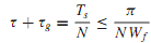
based on the sampling theorem. A time slot is the time per sampling interval that is allowed per message. It is equal to the sum of the sampling-pulse duration τ and separation τg, called the guard time. Thus, we have

692_What is Signal Multiplexing1.png

The time that is required to gather at least one sample of each message is known as a frame, which is Ts, as shown in Figure (d). Now, with a single composite source of the waveform shown in Figure (d) at point A of Figure (a), the time multiplexer of Figure (a) operates beyond A. For Nb-bit encoding, each time slot in the output PCMsignal will have Nb bits of duration,

It is assumed that all sample trains are derived from the same timing source, called a clock, and hence have the same frequency. Instead of using up all frame time for messages, some time is usually allocated for synchronization so that the receiver will know the start times of frames.

1818_What is Signal Multiplexing2.png


Related Discussions:- What is signal multiplexing

Determine the capacitor voltage, Q. In an RLC series circuit excited by a v...

Q. In an RLC series circuit excited by a voltage source v(t), for R = 10 , L = 1 H, and C = 0.1F, determine v(t) if the capacitor voltage vC(t) = 5e -10t V.

Common-drain jfet amplifier, Q. Common-Drain JFET Amplifier? Figure (a)...

Q. Common-Drain JFET Amplifier? Figure (a) shows a CD JFET amplifier in which resistors R 1 , R 2 , and R SS are selected by the bias design, and capacitors CG and CS are chos

Show how a 16-to-1 multiplexer can be obtained, Q. Using two 8-to-1multiple...

Q. Using two 8-to-1multiplexers and one 2-to-1multiplexer, show how a 16-to-1 multiplexer can be obtained in the form of a block diagram.

Electromechanical meters, Electromechanical Meters Electromechanical e...

Electromechanical Meters Electromechanical energy meters are based on the Ferraris Principle (see note in the margin). The working of these meters is explained. Working o

RC coupled transistor amplifier., why we plot graph to find bandwidth is dr...

why we plot graph to find bandwidth is drawn b/w av/avmax v/s frequency not av v/s frequency?

Higher order address bus - pins and signals , Higher order  Address Bus ...

Higher order  Address Bus The 8085 microprocessor  has 8 pins  dedicated to higher order address A15 - A8. These pins  are used to connect  higher  order address bus. These  p

Demand side management, Demand Side Management Demand side management ...

Demand Side Management Demand side management refers to programmes implemented through utilities to modify consumer load profile. Energy efficiency programmes decrease energy

Find the output function y for the logic circuits, Q. Find the output funct...

Q. Find the output function Y for the logic circuits of Figure (a) and (b). An AOI (AND-OR-INVERT) gate is shown in Figure with its two possible realizations. Obtain the output

Write Your Message!

Captcha
Free Assignment Quote

Assured A++ Grade

Get guaranteed satisfaction & time on delivery in every assignment order you paid with us! We ensure premium quality solution document along with free turntin report!

All rights reserved! Copyrights ©2019-2020 ExpertsMind IT Educational Pvt Ltd