What is enhancement mosfets, Electrical Engineering

Assignment Help:

Q. What is Enhancement MOSFETS?

Figure illustrates the cross-sectional structure of an n-channel enhancement MOSFET and its symbol showing as a normally off device when used for switching purposes. When the gate-to-source voltage vGS > 0, an electric field is established pushing holes in the substrate away from the gate and drawing mobile electrons toward it, as shown in Figure (a). When vGS exceeds the threshold voltage VT of the MOSFET, an n-type channel is formed along the gate and a depletion region separates the channel from the rest of the substrate, as shown in Figure (b).With vGS > VT and vDS > 0, electrons are injected into the channel from the heavily doped n+ source region and collected at the n+ drain region, thereby forming drain-to-source current iD, as shown in Figure (b). Note that none of the electrons comes from the p-type portion of the substrate, which now forms a reverse-biased junction with the n-type channel. As the gate voltage increases above VT, the electric field increases the channel depth and enhances conduction. For a fixed vGS and small vDS, the channel has uniform depth d, acting like a resistance connected between the drain and source terminals. The MOSFET is then said to be operating in the ohmic state.

2178_What is Enhancement MOSFETS.png

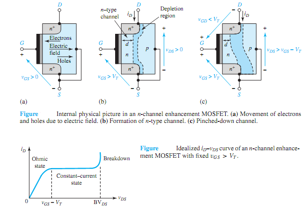
With a fixed vGS >VT , increasing vDS will reduce the gate-to-drain voltage vGD(= vGS - vDS), thereby reducing the field strength and channel depth at the drain end of the substrate.When vDS >(vGS - VT ), i.e., vGD < VT ,a pinched-down condition occurs when the electron flow is limited due to the narrowed neck of the channel, as shown in Figure(c). The MOSFET is then said to be operating in a constant-current state, when iD is essentially constant, independent of vDS.

Figure illustrates the MOSFET behavior explained so far. When vGS ≤ VT , however, the field is insufficient to form a channel so that the iD-vDS curve for the normally off state is simply a horizontal line at iD = 0. The drain breakdown voltage BVDS ranges between 20 and 50 V, at which the drain current abruptly increases and may damage the MOSFET due to heat if operation is continued. The gate breakdown voltage, at about 50 V, may also cause a sudden and permanent rupture of the oxide layer.


Related Discussions:- What is enhancement mosfets

Find internal resistance across terminals, Q. In the Wheatstone bridge circ...

Q. In the Wheatstone bridge circuit shown in Figure, R 1 = 16, R 2 = 8, and R 3 = 40; R 4 is the unknown resistance. RM is the galvanometer resistance of 6 . If no current

Determine thevinin and norton equivalent circuit, Design and simulate by us...

Design and simulate by using multisim software a series voltage regulator to supply 1A to a load at a constant voltage of 9V. The supply voltage to regulator is 15V±10%. The minimu

Interpoles and compensating windings, Interpoles and Compensating Windings:...

Interpoles and Compensating Windings: The most generally used method for aiding commutation is by providing the machine with inter poles, also known as commutating poles, or si

Find the line current after the addition of capacitor bank, Q. Find the lin...

Q. Find the line current after the addition of capacitor bank? A 60-Hz, three-phase motor draws 25 kVA at 0.707 lagging power factor from a 220-V source. It is desired to impro

Flashlight, Why are some flashlights brighter than others? Why is it import...

Why are some flashlights brighter than others? Why is it important that all of the batteries point in the same direction? What is the difference between old batteries and new? What

Low investments in transmission and distribution system, Low Investments in...

Low Investments in Transmission and Distribution System The investment on T&D system in our country has commonly been lower than that on generation. It is hugely believed in

Digital Signal Processing, Can you do a survey paper on Wavelet and Subband...

Can you do a survey paper on Wavelet and Subband Coding? I need 10 pages and I will provide the references.

Define the xor gate - microprocessor, Define the XOR GATE - Microprocessor?...

Define the XOR GATE - Microprocessor? The XOR GATE is a alike to an OR gate except for the instance when all the inputs are high. With a XOR gate when all the inputs are high t

Carrier modulation by digital signals, Q. Carrier Modulation by Digital Sig...

Q. Carrier Modulation by Digital Signals? Digitally modulated signals with low-pass spectral characteristics can be transmitted directly through baseband channels (having low-p

Write Your Message!

Captcha
Free Assignment Quote

Assured A++ Grade

Get guaranteed satisfaction & time on delivery in every assignment order you paid with us! We ensure premium quality solution document along with free turntin report!

All rights reserved! Copyrights ©2019-2020 ExpertsMind IT Educational Pvt Ltd