Transistors:
The transistor can be a high or low resistance device, hence the name, which is derived from TRANSfer resISTOR.
It is used in many switching and amplifier circuits where its resistive properties are controlled by small currents.
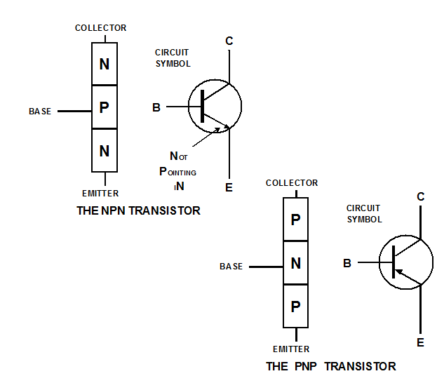
The properties of semi-conductor materials, P and N type, were discussed in Module 4.1.1. A transistor is made up of these materials in the configurations shown in Figure. The circuit symbols for these transistors are also shown.

As can be seen from figure 1, there are two possible types of physical arrangement:
1. The N-P-N transistor, which consists of a thin region of P-type material, sandwiched between two N-type regions.
2. The P-N-P transistor, which consists of a thin region of N-type material, sandwiched between two P-type regions.
The centre region of the device is called the "Base"; one outer region is called the "Emitter", and the other the "Collector". Although the emitter and collector regions are the same type of extrinsic semiconductor (N-type in N-P-N and P-type in P-N-P), they are constructed and doped differently and are not interchangeable on a practical device.
The circuit symbol for both P-N-P and N-P-N are shows in figure. The only difference between them is the direction of the arrowhead on the emitter lead. For either type, the arrowhead indicates the direction of "Conventional" current flow when the base/emitter junction is forward biased (i.e. base +ve with respect to emitter for an N-P-N device, and base -ve relative to emitter for a P-N-P device).