Simulation of a pn junction, Electrical Engineering

Assignment Help:

Simulation of a pn Junction

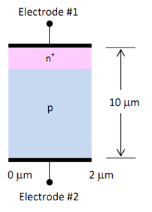
An n+ p junction is fabricated on a p-type silicon substrate with NA = 8×1015 cm-3 . The n+ region has a concentration of ND = 1.5×1018 cm-3 and a junction depth of xj = 1.4 μm. The total device depth is 10 μm (from top to bottom contact).

Use Sentaurus to simulate and view the results for the following conditions:

1. Zero Bias, Uniform Doping Profiles Using uniform doping profiles, verifies the 1D and 2D doping concentration of this junction. Also plot the 1D potential across the junction to estimate the built-in potential and depletion region width. Compare the results with the theoretical values.

You may want to use a non-uniform mesh, which is denser in the top 2 μm of the device.

2. Reverse Bias, Uniform Doping Profiles Simulate the diode under reverse bias. Plot the reverse IV characteristics and extract the breakdown voltage. Compare your result with Figure in the text. What is the maximum electric field in the junction just before breakdown?

2305_Simulation of a pn Junction.png

3. Forward Bias, Uniform Doping Profiles Plot the IV relation for this diode under a forward bias between 0 and 1 V. What allows us to raise the forward bias above 0.7 V? How can this be seen from the simulation output?

Hint: Examine the change in the IV curve with increasing voltage and determine the cause of this change.

4. High Temperature, Uniform Doping Profiles The junction temperature is raised to 580°C. Simulate this junction up to a reverse bias of 12V and a forward bias of 1V. Plot and explain the IV characteristics.

5. Reverse Bias, Gaussian n+ Doping Profiles Using a Gaussian profile for the n+ region with peak concentration of 1.5×1018 cm-3 and junction depth of xj = 0.7 μm, verify the 1D and 2D doping concentration of the junction. Plot the 1D potential across the junction to estimate the built-in voltage and depletion width at equilibrium. Compare Vbi with the theoretical value and compare Vbi and junction width to those from part 2. Also, estimate the minority carrier diffusion lengths Ln and Lp.


Related Discussions:- Simulation of a pn junction

What do you mean by nibble, Q. What do you mean by Nibble? The nibble i...

Q. What do you mean by Nibble? The nibble is a collection of bits on a 4-bit boundary. It would not be a particularly interesting data structure except for two items BCD (binar

Minimized circuit using or and and not gate, Given S(F) = A'B +'C'D + C'D +...

Given S(F) = A'B +'C'D + C'D +'A'B + 'A B + 'A 'C + 'A D + 'A C A. DRAW A MINIMIZED CIRCUIT USING ONLY OR AND NOT GATES (2 input gates) B. WRITE THE WIRE LIST Example of a

Automatic irrigation system on running solar power b, how to upload the pro...

how to upload the program on proteus software by using personal computer

Factors affecting high commercial losses, Factors Affecting High Commercial...

Factors Affecting High Commercial Losses Commercial losses in our country occur mainly because of the following reasons: Incorrect assessment of the energy consum

Matlab simulation, Simulate and compare BER of QPSK system and 4-QAM system...

Simulate and compare BER of QPSK system and 4-QAM system without grey coding Eb/No=0.2.4.6.8.10

Key performance indicators in business, Key Performance Indicators in Busin...

Key Performance Indicators in Business Significance of Key Performance Indicators (KPIs) in the business of power especially within a change environment due to partial deregul

Determine the line-to-line voltage, Q. A one-line diagram of a three-phase ...

Q. A one-line diagram of a three-phase distribution system is given in Figure. Determine the line-to-line voltage at the sending end of the high-voltage feeder when the transformer

Explain the construction of a mosfet, Explain the construction of a MOSFET....

Explain the construction of a MOSFET. Draw the symbols and diagrams of both P-channel and N-channel MOSFET. As JFET and MOSFET also have source, drain and gate. Its gate is ins

DSP-chebyshev, Consider Chebyshev Type I versus Chebyshev Type II (also cal...

Consider Chebyshev Type I versus Chebyshev Type II (also called inverse Chebyshev) Ölters. Which one should be used based on the following criteria? (If there is no difference betw

Switching characteristics during turn off, Switching Characteristics During...

Switching Characteristics During Turn off The techniques  used for turning off a thyristor is known  as  commutation techniques. A  thyristor can be can be  turn off by reducin

Write Your Message!

Captcha
Free Assignment Quote

Assured A++ Grade

Get guaranteed satisfaction & time on delivery in every assignment order you paid with us! We ensure premium quality solution document along with free turntin report!

All rights reserved! Copyrights ©2019-2020 ExpertsMind IT Educational Pvt Ltd