Program implementing the conjugate gradient method, Electrical Engineering

Assignment Help:

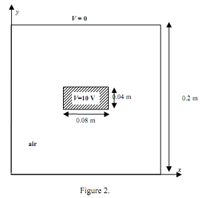
Write a program implementing the conjugate gradient method (un-preconditioned). Solve the  matrix equation corresponding to a finite difference node-spacing, h = 0.02m in x and y directions for the same one-quarter cross-section of the system shown in Figure. Use a starting solution of zero.

(a) Test your matrix using your Choleski decomposition program that you wrote for Question 1 of Assignment 1 to ensure that it is positive definite. If it is not, suggest how you could modify the matrix equation in order to use the conjugate gradient method for this problem.

(b) Once you have modified the problem so that the matrix is positive definite, solve the matrix equation first using the Choleski decomposition program from Assignment 1,and then the conjugate gradient program written for this assignment.

(c) Plot a graph of the infinity norm and the 2-norm of the residual vector versus the number of iterations for the conjugate program.

(d) What is the potential at (x,y) = (0.06, 0.04), using the Choleski decomposition and the conjugate gradient programs, and how do they it compare with the value you computed in Question 2(b) above. How do they compare with the value at the same (x,y) location and for the same node spacing that you computed in Assignment 1 using SOR.

(e) Suggest how you could compute the capacitance per unit length of the system from the finite difference solution.

506_Compute the capacitance.png


Related Discussions:- Program implementing the conjugate gradient method

Bode plot, Hai.. i have been given a open loop transfer function to draw a...

Hai.. i have been given a open loop transfer function to draw a bode plot with a particular K value and they asked me to find the value of K for which the phase margin becomes 45d

Find the resistor values of rc, Apply the rule-of-thumb dc design presented...

Apply the rule-of-thumb dc design presented in this section for a silicon npn BJT with β = 70 when the operating Q point is defined by I CQ = 15 mA and I BQ = 0.3 mA, with a dc s

Intrinsic material, Int r insic Material A perfect semicon...

Int r insic Material A perfect semiconductor crystal with no impurities or lattice defects. No carriers at 0 K, since the valence band is completely full and t

Determine l and c of the band reject filter circuit, Q. Determine L and C o...

Q. Determine L and C of the band reject filter circuit of Figure to have a center frequency of 100 kHz and a bandwidth of 5 kHz. Also find the Q of the filter.

Instrument, Differentiate between dual beam and dual trace oscilloscope

Differentiate between dual beam and dual trace oscilloscope

Network theorems.., how to calculate voltage when 3 voltage sources are giv...

how to calculate voltage when 3 voltage sources are given?

Explain the power chart, Explain the Power Chart The phasor diagram sho...

Explain the Power Chart The phasor diagram shown in Figure with the x and y axes added, as shown. This diagram may be converted to a 'power chart' by multiplying each phasor in

Write Your Message!

Captcha
Free Assignment Quote

Assured A++ Grade

Get guaranteed satisfaction & time on delivery in every assignment order you paid with us! We ensure premium quality solution document along with free turntin report!

All rights reserved! Copyrights ©2019-2020 ExpertsMind IT Educational Pvt Ltd