Output characteristics , Other Engineering

Assignment Help:

OUTPUT CHARACTERISTICS:

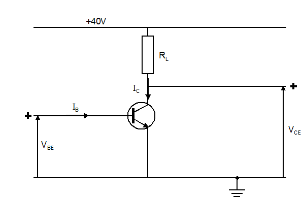
Figure shows a "Common Emitter" amplifier stage.
2319_OUTPUT CHARACTERISTICS.png

Common Emitter Amplifier Stage

With no base/emitter bias applied, there will be no collector current flowing.  The output voltage VCE will be equal to the supply voltage (40V).  As the collector current  IC flows through resistor RL there will be a voltage drop (IC x RL) across the resistor.  The collector voltage will depend upon the collector current i.e.  40V minus IC x RL  volts.

If  IC  is zero, then VCE must be 40v. VCE  could be reduced to zero by a value of  IC  of 40/RL amperes.  If we assume RL to have a value of 18 ohms, then VCE will be zero for an IC of approximately 2.2 amperes.

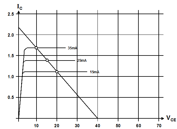
Figure shows a graph plotting collector current against collector/emitter voltage
for different values of base current.


The straight line from the collector/emitter voltage axis to the collector current axis is the "Load Line" and indicates the only values of VCE and IC which are possible for that circuit.  Obviously, if a different value of RL is used, we would get a different load line with a different slope.
1834_OUTPUT CHARACTERISTICS1.png

For amplifiaction to take place we must first apply an initial bias voltage to the base.  With 1.3 VBE applied the IB will be 25mA giving an IC of 1.4A which would produce an output of 15V (VCE).  If we now apply a sinusoidal input signal of 0.6V, the base current would vary between 15 --35mA, which in turn would vary the IC between 1.1 - 1.7A, giving a voltage output between 10 - 20V.

This produces an amplifier gain of 0.6A/25mA = 30.  Figure shows the voltage/current waveforms of these variations.


Related Discussions:- Output characteristics

Active clearance control system, Active clearance control system The sy...

Active clearance control system The system provides fan discharge air for cooling the core compartment and the low-pressure turbine case. At low altitudes the core engine requ

Logic gate - nand gate, NAND Gate; When constructing a NAND gate using ...

NAND Gate; When constructing a NAND gate using transistors as the switching devices, the output often represents the 'inversion' of the "AND" gate. Figure 4 shows an example o

Effects of temperature and altitude on engine, Effects of Temperature and A...

Effects of Temperature and Altitude. Cold and/or Low On cold days the air density will increase. If the engine has a ‘part throttle rating' and the throttle is advanced to

Calculate pi for infinite series, Write a program to calculate from the i...

Write a program to calculate from the infinite series: Print a table showing the value of approximated by one term, two terms, three terms, four terms, and so on from th

X rays., how x rays are produced?

how x rays are produced?

How does or gate work, Expertsmind.com  brings you unique solution in Elec...

Expertsmind.com  brings you unique solution in Electrical Engineering   How does OR gate work? An 'OR' gate is like two or more switches positioned in parallel.

Write Your Message!

Captcha
Free Assignment Quote

Assured A++ Grade

Get guaranteed satisfaction & time on delivery in every assignment order you paid with us! We ensure premium quality solution document along with free turntin report!

All rights reserved! Copyrights ©2019-2020 ExpertsMind IT Educational Pvt Ltd