The modes are determined by the contents of the control register, whose format is given in Figure These modes are:
Mode 0: If a group is in mode 0, it is divided into 2 sets. For group A these sets are port A ad the upper 4four bits of port C, and for group B they are in port B ad the lower 4 bits of port C. every set can be used for inputting or outputting, but not both. Bits D0, D1, D2, and D4 in the control register indicate which sets are for input and which are for output.
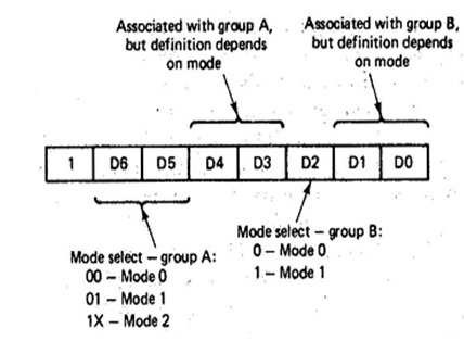
These bits are associated with the sets as follows: D4 - Port A.
D3 - Upper half of port C. D1 - Port B.
D0 - Lower half of port C.
If a bit is 0, then the corresponding set is utilize for output; if it is 1, the set is for input.
Mode 1: When group A is in this mode port A is utilized for input or output according to bit D4 (d4=1 indicates input), and the upper half of ports C is utilized for control signals and handshaking. For inputting, the 4 MSBs of port C are assigned the following symbols and definition:
PC4 STBA A 0 applied to this pin causes PA7-PA0 to be latched, or "strobe," into port A.
PC5 IBFA indicates that the input buffer is full. It is one when port A contains data that have not yet been input to the CPU. When it is 0 is on this pin the device can Input a new byte to the interface.
PC6, PC7 May be used to output control signals to the device or input status from the device. If D3 of the control register is 0, they are for outputting control signals; or else, they are for inputting status. For outputting
PC4, PC5 Serve the same purpose as described above for PC6 and PC7.
PC7 OBFA indicates that the output buffer is full. It outputs a 0 to the device when
PC6
ACKA port A is outputting new data to be taken by the device.
Device puts a zero on this pin when it accepts data from port A.
In mode 1, PC3 is indicating INTERA and is linked with group A. It is utilized as an interrupt request line and is tied to 1 of the IR line in the system bus. When it is inputting to port A, this pin becomes one when new data are put in port A (for instance, it is controlled by PC4) and it is cleared when the CPU takes the data. For output, this pin is set to one when the contents of port A are taken by the device as cleared when new data are sent from the CPU. If group B is in mode 1, port B is output from or input to according to bit D1 of the control register (D1=1 denote input). For input, PC1 and PC2 are specify IBFB and STBB, respectively, and serve the similar purposes for group B as STBAAND IFBA do for group A. likewise, for output PC1 and PC2 are indicated OBFB and ACKB. PC0 becomes INTERB and its utilized is analogous to that of INTRA. The interrupt make able for group A is controlled by clearing integral flags or setting. clearing or Setting these flags is simulated by or clearing and setting PC4, for input, or PC6, for output, by using a Reset/set instruction. Likewise, the interrupt allow for group B is controlled by set/clear of PC2 for input and output both.
Mode 2: This mode applies just to group A, although it also utilized PC3 for making interrupt requests. In the mode 2, the port A is a bidirectional port and the 4 MSBs of port C are defined as follows:
PC4
PC5 STB
IBFA A 0 on this line causes the data on PA7 - PA0 to be strobe into port A.
Becomes one when port A is filled with new data from lines PA7 - PA0 and
It is cleared that when these data are taken by the CPU.
PC6 ACKA denotes that the device is ready to accept data from PA7-PA0.
PC7 OBFA Becomes 0 when the port A is filled with new data from the CPU and is set to
1 when data are taken by the device.
While group A is in mode 2, group B might be in either mode 0 or mode 1. However, if group B is mode 0, only PC2 - PC0 can be used for input or output because group A has borrowed PC3 to use as an interrupt request line. Usually, if group A is in mode, PC2 -PC0 would be linked to control and status pins on the device attached to the port A lines. Port B can utilize for this purpose.
In all 3 modes port C reflects the signals on PC7 - PC0 and may be read with an IN instruction.