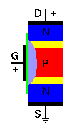
Mechanical Structure of Depletion Type MOSFET
The mechanical structure of this type of device is displayed in figure. In an IC, we would locate two n-type regions side by side in a p-type area and then place the gate in between the n-type regions. Though, the important region still contains the two n-type regions and the p-type area in between them.
Without applied bias, we have what amounts to an npn transistor without base connection. The two n-type regions are electrically separate and isolated from each other. Although with a voltage applied in between the two n-type regions, there is no channel present and no current flow.
Whereas we still apply the usual positive voltage to the drain with respect to the source, this time we will as well apply a positive voltage to the gate region. This comprises the effect of attracting free electrons in the direction to the gate. The larger the positive gate voltage, the wider its electric field and the much more free electrons it will attract.
You may not think this would have any influence on the p-type region, in which the majority current carriers are holes. Though, there are some free electrons here also. Additionally, the source junction is forward biased, thus the positive gate voltage can attract electrons across this junction towards the gate.
The net result is that the electrons attracted in the direction to the gate actually improve a channel within the p-type region, as displayed in figure. This is a channel that is made up of free electrons, and actually bridges the gap in between source and drain. Now we have a channel that can conduct current from source to drain by the device.