Interrupt system based on 8259 a-microprocessor, Assembly Language

Assignment Help:

Interrupt System Based on Single 8259 A

The 8259A is contained in a 28-pin dual-in-line package that need only a + 5-V supply voltage.  Its organization is shown in given figure along with its associates to a maximum mode system. Its pins (other than the ground pins and supply voltage) are defined as follows:

D7-DO - For communicating with the CPU over the data bus. On a few systems bus drivers might be required, but on the other systems direct connections can be used.

INT - It is used to send interrupt request signals to the CPU.

INTA - it is used to receive interrupt acknowledge signals from the CPU. The 8259A consider that an acknowledgment consists of two negative pulses, thus making it is compatible with 8086/8088 systems.

RD - it is used to signal the 8259A that it is to place the contents of the IRR ,ISR, or IMR, register or a priority level on the data bus. These possibilities is placed on the bus depends on the state of the 8259A and is discussed below.

1448_8259 A.jpg

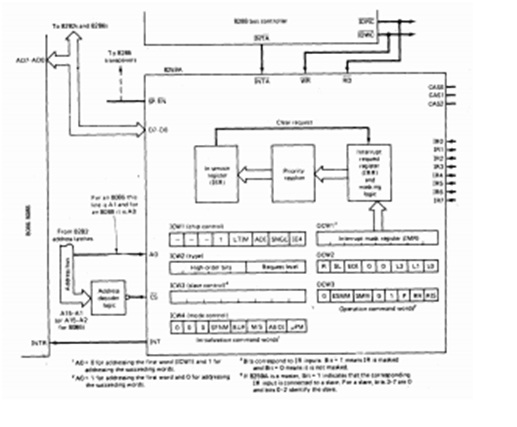
WR - To signal the 8259A that it is to receive data from the data bus and us the data to set the bits in the command words.

CS - For indicating that the 8259A is being accessed. This pin is linked to the address bus through the decoder logic that compares the high-order bits of the address of the 8259A with the address presently on the address bus.  Input to this pin may be combined with S2 to give the ready signal.

AO - For indicating which port of the 8259A is being accessed.  2 addresses might be booked in the I/O address space for each 8259A in the system.

IR7-IRO - For receiving interrupt requests from I/O interfaces or other 8259As mentioned to as slaves.

CAS2-CASO - To recognize a specific slave device.

SP/EN  - For 1 of 2 purposes; either as an input to decide whether the 8259A is to be either as a slave (SP/EN = 0) or a master (SP/EN = 1) as an output to disable the data bus transceivers when data are being transferred from the 8259A to the CPU. Whether the SP/EN pin is utilized as an input or output depends on the buffer mode discussed below.


Related Discussions:- Interrupt system based on 8259 a-microprocessor

Assignment, You have to write a subroutine (assembly language code using NA...

You have to write a subroutine (assembly language code using NASM) for the following equation.

Compute the fibonacci sequence - assembly program, Compute the Fibonacci se...

Compute the Fibonacci sequence - assembly program: Problem: Fibonacci   In this problem you will write a program that will compute the first 20 numbers in the Fibonacci sequ

The pin diagram of 8088-microprocessor, Pin diagram of 8088 : The pin ...

Pin diagram of 8088 : The pin diagram of 8088 is shown in given figure. Most of the 8088 pins and their functions are exactly similar to the corresponding pins of 8086.  Hence

Assembly language programs-microprocessor, Assembly Language Example Progra...

Assembly Language Example Programs We studied the entire instruction set of 8086/88, pseudo-ops and assembler directives. We have explained the process of entering an assembly

Project 1: Text Conversion, I need a text conversion program written in ass...

I need a text conversion program written in assembly language

Pin functions of 8086-microprocessor, Pin functions for the minimum mode o...

Pin functions for the minimum mode operation of 8086 are following: 1) M/I/O -Memory/IO: This is a status line logically equivalent to S2 in maximum mode. When it is low, it

Write an assembly program to find out largest number, Program :  Write an...

Program :  Write an assembly program to find out the largest number from a given unordered array of 8-bit numbers that stored in the locations starting from a known address. S

8088 timing system diagram-Microprocessor, 8088  Timing System Diagram ...

8088  Timing System Diagram The 8088 address/data  bus is divided  in 3 parts (a) the lower 8 address/data  bits, (b) the middle 8 address bits, and (c) the upper 4 status/

Opcode-microprocessor, Opcode : The opcode generally appear in the firs...

Opcode : The opcode generally appear in the first byte.but in a few instructions, a register objective is in the first byte and few other instructions may have their 3-bits of

Dq-dt-assemblers directive-microprocessor, DQ:   Define  Quad word:-  Th...

DQ:   Define  Quad word:-  This directive is taken in use to direct the assembler to reserve 4 words (8 bytes) of memory for the specified variable and can initialise it having

Write Your Message!

Captcha
Free Assignment Quote

Assured A++ Grade

Get guaranteed satisfaction & time on delivery in every assignment order you paid with us! We ensure premium quality solution document along with free turntin report!

All rights reserved! Copyrights ©2019-2020 ExpertsMind IT Educational Pvt Ltd