Internal Architecture of Microprocessor :
The architecture of 8086 provides a number of improvements over 8085 architecture. It supports a, a set of 16-bit registers ,16-bit ALU and provides, a rich instruction set, powerful interrupt structure, segmented memory addressing capability, fetched nstruction queue for overlapped fetching and execution etc. The internal block diagram, denoted in given figure describes the whole organization of different units inside the Chip.
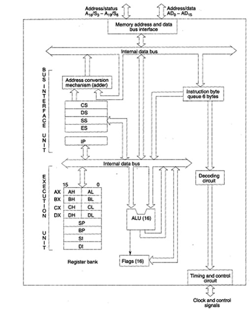
Figure: 8086 Architecture
The whole architecture of 8086 may be divided into 2 parts (a) Execution Unit (EU). And (b) Bus Interface Unit (BIU) The bus interface unit have the circuit for physical address calculations and a prerecording instruction byte queue (6 bytes long). The bus interface unit makes the system bus signals available for external interfacing of the devices. Alternatively this unit is responsible for establishing communications with peripherals and external devices by including memory via the bus. As already stated, the8086 addresses a segmentedmemory. The whole physical address which is 20-bits long is generated by using segment and offset registers, each 16-bit long.
For generating a physical address from contents of these2 registers, the content of a segment register also known as segment address is shifted left bit-wise 4 times and to this result, content of an offset register also known as offset address is added, to generated a 20-bit physical address. For instance, if the segment address is 1005H and the offset is 5555H, then the physical address is calculated as below.
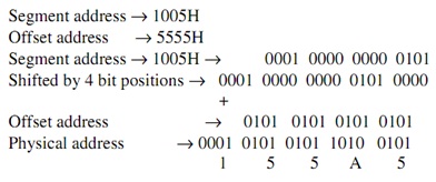
So the segment addressed by the segment value 1005H can have offset values from 0000H to FFFFH within it, for example maximum 64K locations can be accommodated in the segment. Thus the segment register denotedthe base address of a specificsegment, while the offset indicates the distance of the required memory location in the segment from the base address. Since the offset is a 16-bit number, each segment may have a maximum of 64K locations. The bus interface unit has a separate adder to perform this procedure for obtaining a physical address whereas addressing memory. The segment address value is taken from an proper segment register depending upon whether code, data or stack are to be accessed, when the offset can be the content of BX, IP, SI, SP, DI or an immediate 16-bit value, depending upon the addressing mode.
In case of 8085, once the opcode is decodedand fetched, the external bus remains free for some time, while the processor internally executes the instruction. This time slot is used in 8086 to gain the execution cycles andoverlapped fetch. While the fetched instruction is executed internally, the external bus is utilized to fetch the machine code of the next instruction and arrange it in a queue called as pre decoded instruction byte queue. It is 6 bytes long, first-in first-out structure. The instructions from the queue are taken for decoding sequentially. Once a byte is decoded, the queue is rearranged by pushing it out and the queue status is examined for the possibility of the next opcode fetch cycle. While the opcode is fetched by the execution unit (EU) ,the bus interface unit (BIU), executes the previously decoded instruction concurrently. The BIU along with the execution unit (EU) thus forms a pipeline. The bus interface unit thus manages the total interface ofexecution unit with memory and I/O devices, of course, under the control of the timing and control unit.
The execution unit have the register set of 8086 except IPand segment registers. It has a 16-bit ALU, able to perform logic andarithmetic operations. The 16-bit flag register reflects the results of execution by the ALU. The decoding unit decodes the opcode bytes issued from the instruction byte queue. The control andtiming unit derives the essential control signals to execute the instruction opcode received from the queue, depending on the information madeavailable by the decoding circuit. The execution unit can pass the results to the bus interface unit for storing them in memory.