Illustrate simple ALU organisation, Computer Engineering

Assignment Help:

Q. Illustrate Simple ALU Organisation?

An ALU comprises circuits which perform data processing micro-operations. Though how are these ALU circuits used in conjunction of other registers and CU? The simplest organisation in this respect for fixed point ALU was proposed by John von Neumann in his IAS computer design.

2140_Illustrate Simple ALU Organisation.png

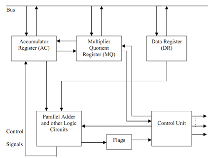
Figure: Structure of a Fixed point Arithmetic logic unit

The above structure has 3 registers AC, MQ and DR for data storage. Let's presume that they are equal to one word each. Please consider that Parallel adders and other logic circuits (these are the arithmetic, logic circuits) have two inputs and just one output in this figure. It suggests that any ALU operation at most can have two input values and will produce single output along with other status bits. In the current case the two inputs are AC and DR registers whereas output is AC register. AC and MQ registers are usually used as a single AC.MQ register. This register is capable of right or left shift operations. A number of the micro-operations which can be defined on this ALU are:

Addition            :  AC ← AC + DR

Subtraction        :  AC ← AC - DR 

AND                 :  AC ← AC ^ DR

OR                  :  AC ← AC   DR

Exclusive OR    :  AC ← AC (+) DR

NOT                 :  AC ← AC

In this ALU organisation division and multiplication were implemented employing shift-add/subtract operations. MQ (Multiplier-Quotient register) is a special register used for implementation of division andmultiplication. We aren't providing details of how this register can be used for implementing division and multiplication algorithms. For more details on these algorithms please refer to further readings. An example of this type of algorithm is Booth's algorithm and you should refer to it in further readings.  

For division or multiplication operations DR register stores the divisor or multiplicand respectively. The result of division or multiplication on applying certain algorithm can finally be attained in AC.MQ register combination. These operations can be signified as:

Multiplication   :  AC.MQ ← DR × MQ

Division           :  AC.MQ ← MQ ÷ DR

DR is another significant register which is used for storing second operand. Actually it acts as a buffer register that stores the data brought from memory for an instruction. In machines where we have general purpose registers any of the registers can be utilized like AC, MQ and DR.


Related Discussions:- Illustrate simple ALU organisation

C++, minimum self program

minimum self program

Write a bash shell script, Write a BASH/C shell script which takes name of ...

Write a BASH/C shell script which takes name of one or more files as a command line argument, and prints the following information for each file: owner, number of words in the file

Explain dead code elimination, Explain briefly Dead code Elimination of the...

Explain briefly Dead code Elimination of the commonly used code optimization techniques Dead code Elimination: Code which is unreachable or which does not influence the pr

Illustrate the cache memory operation, Q. Illustrate the Cache Memory Opera...

Q. Illustrate the Cache Memory Operation? It comprises a copy of a part of main memory contents. When a program is running and CPU tries to read a word of memory (instruction o

I2c protocol bus , I²C TECHNOLOGIES The I2C protocol bus is two bi-dire...

I²C TECHNOLOGIES The I2C protocol bus is two bi-directional wires, serial data (SDA) and serial clock (SCL), that transmit information between the devices connected to the bus.

Software engineering - layered technology, S oftware Engineering - Layered...

S oftware Engineering - Layered Technology Although various authors have developed personal definitions of software engineering, a definition given by Fritz Bauer at the semin

How many ram chips are required for memory of 2048 bytes, How many 128 × 8 ...

How many 128 × 8 RAM chips are required to provide a memory capacity of 2048 bytes. Ans. Available here RAM chips = 128 x 8 Required the memory capacity    = 2048 x 8 No. of chip

What is the bios full form, BIOS - Basic Input Output System, Power On ...

BIOS - Basic Input Output System, Power On Self Test (POST) and Loading Bootloader from the Hard disk drive Boot Sector is being completed by BIOS. It started the system for

Determine by which digits are represented in dtmf phone, In a DTMF phone, d...

In a DTMF phone, digits are represented by: (A)  Orthogonal frequencies. (B)  Orthogonal Phases. (C)  Orthogonal codes. (D)  Orthogonal pulses. Ans: Di

Wireless Networking, Suppose you work in a network security company, and yo...

Suppose you work in a network security company, and you need to prepare a survey report of a particular security issue of wireless networking. To start with, select an area of wire

Write Your Message!

Captcha
Free Assignment Quote

Assured A++ Grade

Get guaranteed satisfaction & time on delivery in every assignment order you paid with us! We ensure premium quality solution document along with free turntin report!

All rights reserved! Copyrights ©2019-2020 ExpertsMind IT Educational Pvt Ltd