Illustrate nodal-voltage method, Electrical Engineering

Assignment Help:

Q. Illustrate Nodal-Voltage Method ?

A set of node-voltage variables that implicitly satisfy the KVL equations is selected in order to formulate circuit equations in this nodal method of analysis. A reference (datum) node is chosen arbitrarily based on convenience, and from each of the remaining nodes to the reference node, the voltage drops are defined as node-voltage variables. The circuit is then described completely by the necessary number of KCL equations whose solution yields the unknown nodal voltages from which the voltage and the current in every circuit element can be determined. Thus, the number of simultaneous equations to be solved will be equal to one less than the number of network nodes. All voltage sources in series with resistances are replaced by equivalent current sources with conductances in parallel. In general, resistances may be replaced by their corresponding conductances for convenience.Note that the nodal-voltagemethod is a generalmethod of network analysis that can be applied to any network.

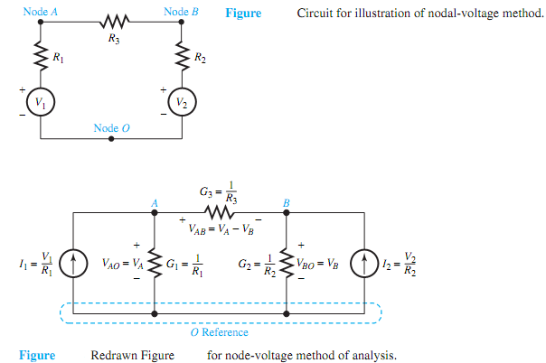
Let us illustrate the method by considering the simple, but typical, example shown in Figure 2.2.1. By replacing the voltage sources with series resistances by their equivalent current sources with shunt conductances, Figure 2.2.1 is redrawn as Figure 2.2.2, in which one can identify three nodes, A, B, and O.

Notice that the voltages VAO, VBO, and VAB satisfy the KVL relation:

VAB + VBO - VAO = 0, or VAB = VAO - VBO = VA - VB

where the node voltages VA and VB are the voltage drops from A to O and B to O, respectively. With node O as reference, and with VA and VB as the node-voltage unknown variables, one can write the two independent KCL equations:

1470_Illustrate Nodal-Voltage Method.png

829_Illustrate Nodal-Voltage Method1.png


Related Discussions:- Illustrate nodal-voltage method

Determine the transfer function in notch network, Q. The twin-tee or notch ...

Q. The twin-tee or notch network shown in Figure is often used to obtain band-reject characteristics. (a) Determine the transfer function V 2 /I 1 . (b) Find the angular freq

Explain the high-frequency response of fet amplifier, Q. Explain the high-f...

Q. Explain the high-frequency response of FET amplifier?  The analysis for the high frequency response of the FET amplifier is almost the same as that of the BJT amplifier. The

Explain the and gates - microprocessor, Explain the AND GATES - Microproces...

Explain the AND GATES - Microprocessor? The AND GATE has a logic 1 or high output if the entire inputs are high. The boolean and symbol expression for a 3-input AND gate is sho

What do you mean by magnetic circuits, Q. What do you mean by Magnetic circ...

Q. What do you mean by Magnetic circuits? A magnetic circuit provides a path for magnetic flux, just as an electric circuit provides a path for electric current.Magnetic circui

Define electric current, Define Electric current If an electric pressur...

Define Electric current If an electric pressure or voltage is applied across any material there is a tendency for electrons to move in a certain direction. This movement of fre

Extended industry standard architecture, How is EISA bus different from ISA...

How is EISA bus different from ISA bus? The Extended Industry Standard Architecture (EISA): it is a 32 bit modification to the ISA bus. Since computers became larger and had wi

Integrated circuit components, You are required to design and document the ...

You are required to design and document the hardware design for Lift Control Unit (LCU) as required by the questions/specification in section 2 above, based on a 68HC12D60 microcon

What is the direction of a line of flux, What is the Direction of a line of...

What is the Direction of a line of flux The direction of a line of flux is from the north pole to the south pole on the exterior of the magnet and is then supposed to continue

What is meant by biasing transistor, Q. What is meant by biasing transistor...

Q. What is meant by biasing transistor? The purpose of dc biasing of transistor is to obtain a certain dc collector current at a certain dc collector voltage. These values of c

Nor gate - introduction to microprocessors , NOR Gate NOR means NOT OR ...

NOR Gate NOR means NOT OR . it complements the  output  of an OR  gate.  The symbol  of Nor  gate in fig. (a) shows that a Nor  gate  comprises  of an OR  gate followed  by a N

Write Your Message!

Captcha
Free Assignment Quote

Assured A++ Grade

Get guaranteed satisfaction & time on delivery in every assignment order you paid with us! We ensure premium quality solution document along with free turntin report!

All rights reserved! Copyrights ©2019-2020 ExpertsMind IT Educational Pvt Ltd