Forward bias
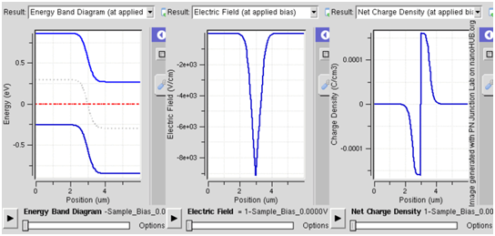
In forward bias, the p-type is linked with the positive terminal and the n-type is linked with the negative terminal.In forward bias mode the PN junction operation displaying reducing depletion width. Both p and n junctions are doped at a 1e15/cm3 doping level, directing to built-in potential of ~0.59V. Decreasing depletion width can be inferred from the shrinking charge profile, since fewer dopants are exposed with increasing forward bias.
With a battery connected this manner, the holes in the P-type region and the electrons in the N-type region are pushed in the direction of the junction. This decreases the width of the depletion zone. To the P-type material repels the holes the positive charge is applied, whereas the negative charge applied to the N-type material repels the electrons. Since electrons and holes are pushed in the direction to the junction, the distance between they get decreases. This lowers barrier in potential. With rising forward-bias voltage, the depletion zone ultimately becomes thin sufficient that the zone's electric field can't counteract charge carrier motion across the p-n junction, therefore reducing electrical resistance. The electrons that cross the p-n junction into the P-type material (or holes that cross into the N-type material) will diffuse in the near-neutral region. Hence, the amount of minority diffusion in the near-neutral zones ascertains the amount of current that may flow through the diode.
Single majority carriers (electrons in N-type material or holes in P-type) can flow via a semiconductor for a macroscopic length. With keep this in mind, refer the flow of electrons across the junction. The forward bias origins a force on the electrons pushing them from the N side toward the P side. With forward bias, the depletion region is enough narrow which electrons can cross the junction and inject into the P-type material. Though, they do not carry on to flow through the P-type material indefinitely, since it is energetically favorable for them to recombine with holes. The average length an electron travels via the P-type material before recombining is termed as the diffusion length, and it is commonly on the order of microns.
Even though the electrons penetrate just only a short distance into the P-type material, the electric current caries on uninterrupted, since holes (the majority carriers) start to flow in the reverse direction. The whole current (the sum of the electron and hole currents) is constant in space, since any variation would cause charge buildup over time (this is current law of Kirchhoff). The flow of holes from the P-type region into the N-type region is closely analogous to the flow of electrons to P from N (electrons and holes swap roles and the signs of all currents and voltages are reversed).
Hence, the macroscopic picture of the current flow via the diode includes electrons flowing via the N-type region toward the junction, holes flowing by the P-type region in the opposite direction toward the junction, and the two species of carriers continually recombining in the vicinity of the junction. The electrons and holes travel in reverse directions, but they as well have opposite charges, thus the overall current is in similar direction on both sides of the diode, as needed.