Fixed and adaptive - optimal filtering, Electrical Engineering

Assignment Help:

Optimal Filtering

1389_Fixed and Adaptive.png

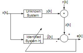
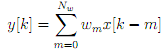
A system identi?cation structure is shown in Figure 1. The discrete-time signal [ ] forms the input to an unknown system represented by a moving average, FIR, ?lter with parameters, {ω01 ωn} . The output of the unknown system is given by

466_Fixed and Adaptive1.png

This can be represented more concisely in vector notation as

1891_Fixed and Adaptive2.png

where ω and x[k] are Nw + 1 element column vectors, underlines are used to denote vector quantities and the superscript (·)T represents a vector transpose.

A noise signal n[k] is added at the output of the system to yield a realistic measured output signal z[k]. An optimum ?lter is to be designed which operates on the input signal x[k] and measured output signal z[k] to yield the closest match to the unknown system. The optimum ?lter is assumed to be a moving average ?lter with the same number of parameters as the unknown system, i.e. opt.

This problem arises in many applications, for example control of some machinery plant, or of acoustic and electrical echoes in telecommunications. The Wiener solution is found by minimising the mean-square error between z[k] and y[k], where y[k] is the output of the optimum ?lter driven by x[k]. The circum?ex is used to denote that the output of the optimum ?lter is an estimate of the output of the unknown system.

If x[k]and n[k] are assumed to be uncorrelated stationary random discrete signals then the mean square error is de?ned as

2274_Fixed and Adaptive3.png

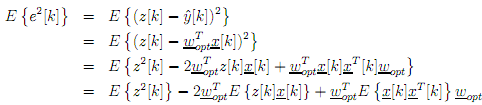
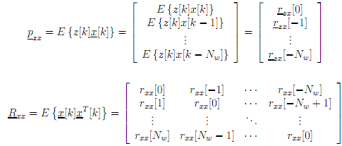
where {·} is the statistical expectation operation, which to a ?rst approximation can be considered to be an average. The right hand side of equation (1) contains a vector of crosscorrelation components and a matrix of autocorrelation components, i.e.

555_Fixed and Adaptive4.png

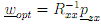
Differenting equation (1) with respect to opt and setting the result to zero yields the optimum Wiener ?lter solution which is given by

596_Fixed and Adaptive5.png


Related Discussions:- Fixed and adaptive - optimal filtering

Jfet ampli?er circuit, Q. For the CS JFET ampli?er circuit of Figure, R D ...

Q. For the CS JFET ampli?er circuit of Figure, R D = 2k and R L = 3k. The JFET with ro = 15 k has a voltage gain A v1 =-4.5 when the entire source resistance is bypassed. Fin

Use delta-wye transformation for network reduction, 1555_Use delta-wye tran...

1555_Use delta-wye transformation for network reduction.png what is the solution to this particular problem?

Carrying out repairs on lt and ht switch gear, Precautions to be taken in c...

Precautions to be taken in carrying out repairs on HT and LT switch gear? Ans: The following precautions to be taken in carrying out repairs on LT and HT switch gears. a

Find the turns ratio of the ideal transformer, Q. Consider an amplifier as ...

Q. Consider an amplifier as a voltage source with an internal resistance of 72 . Find the turns ratio of the ideal transformer such that maximum power is delivered when the amplif

What are the duties of sub-station operator, What are the Basic Duties of S...

What are the Basic Duties of Sub-Station Operator? Ans: Sub station operator is responsible for safe and proper operation of all electrical equipments in sub-station. He co

Determine the laplace transform of the waveform, Q. Determine the Laplace t...

Q. Determine the Laplace transform of the waveform shown in Figure.

Three-phase Portable Bench Power Supply, hi can you help me to create a dc...

hi can you help me to create a dc to 3 phase ac circuit which can exceed at any point: 50V and 20A and 400W maximum. The output should be variable from about 0 – 25V per phase, wi

Calculate the approximate donor binding energy, Calculate the approximate d...

Calculate the approximate donor binding energy Calculate the approximate donor binding energy for Si (r = 11.7,m x n = 1.18 m 0 ) Solution: From E= m * n q 4 / 2(4 πε 0

Why biasing in necessary in transistor, (a) Describe why ordinary junction ...

(a) Describe why ordinary junction transistor is known as bipolar. (b) Describe working of NPN transistor as common Base configuration. Describe working of NPN transistor in

Circuit symbols for mosfet, Circuit Symbols for MOSFET A range of symb...

Circuit Symbols for MOSFET A range of symbols are employed for the MOSFET. The basic design is usually a line for the channel along with the source and drain leaving it at rig

Write Your Message!

Captcha
Free Assignment Quote

Assured A++ Grade

Get guaranteed satisfaction & time on delivery in every assignment order you paid with us! We ensure premium quality solution document along with free turntin report!

All rights reserved! Copyrights ©2019-2020 ExpertsMind IT Educational Pvt Ltd