Find the voltage , Electrical Engineering

Assignment Help:

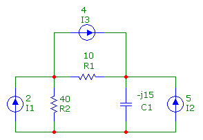
1. Find the current through each component, in polar form, using mesh analysis. The source voltages are rms with an angle of 0 degrees.

1782_circuit.png

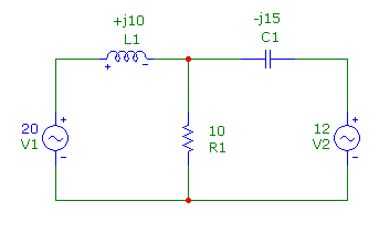
2. Find the current through each component, in polar form, using mesh analysis. The source voltages are rms with an angle of 0 degrees.

1468_circuit 1.png

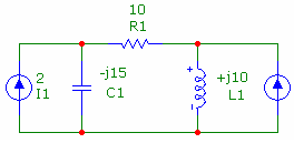
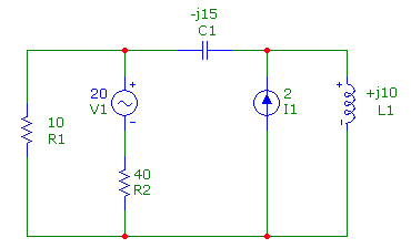
3. Find the voltage across each component, in polar form, using nodal analysis. The source currents are rms with an angle of 0 degrees.

203_circuit 2.png

4. Find the voltage across each component, in polar form, using nodal analysis. The source currents are rms with an angle of 0 degrees.

2198_circuit 3.png

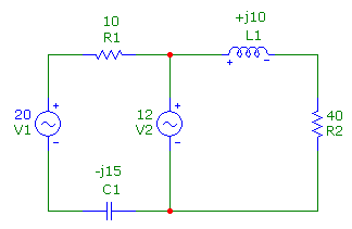
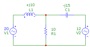
5. Perform some kind of source conversion and use mesh or nodal analysis to find the current through R1 or the voltage across R1. The source values are rms and at 0 degrees.

178_circuit 4.png

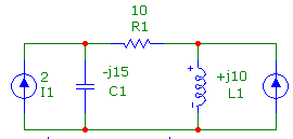
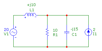
6. Find the current through each component, in polar form, using superposition analysis. The source voltages are rms, at 0 degrees.

821_circuit 5.png

7. Find the current through each component, in polar form, using superposition analysis. The source values are rms, at 0 degrees.

593_circuit 6.png

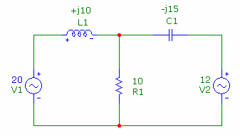
8. Find the voltage across R1, in polar form, using superposition analysis. The source voltages are rms, at 0 degrees.

1364_circuit 7.png

9. Find the current through R1, in polar form, using superposition analysis. The source currents are rms, at 0 degrees.

1934_circuit 8.png


Related Discussions:- Find the voltage

Explain the effect of feedback on amplifier bandwidth, Q. Explain the effec...

Q. Explain the effect of feedback on amplifier bandwidth? The bandwidth of an amplifier is defined as the range of frequencies for which the gain remains constant.The gain -ban

Delay time - power semiconductor devices , Delay time ( t d ) Initiall...

Delay time ( t d ) Initially a thyristor  remains  in forward  blocking  stat when  anode to cathode forward  voltage  is applied  and gate  to cathode circuit is opened. As t

Complete the timing diagram for counter, Q. When the J and K inputs of a JK...

Q. When the J and K inputs of a JKFF are tied to logic 1, this device is known as a divide-by-2 counter. Complete the timing diagram shown in Figure for this counter.

Why is an emitter bypass capacitor in amplifier, Q.  Why is an emitter bypa...

Q.  Why is an emitter bypass capacitor used in an RC coupled amplifier? If an emitter resistor Re is used for self-bias in an amplifier and if it is desired to avoid the degene

Can you explain twos complement division, Q. Can you explain twos Complemen...

Q. Can you explain twos Complement Division? 2's complement division is repeated 2's complement subtraction. The 2's complement of the divisor is calculated, and then added to

Diode current -zener region, Diode current: Zener region: when the r...

Diode current: Zener region: when the reverse biased voltage is increase to a very high value then a point is reached where will is suddenly going a very high value. Th

Explain about the typical embedded system hardware unit, Explain about the ...

Explain about the typical embedded system hardware unit. Typical Embedded System Hardware Unit: Program Flow and data path Control Unit (CU): comprises a fetch unit for fetc

Transfer function of radiator, hi, i want to know the transfer function of ...

hi, i want to know the transfer function of a radiator

Determine the open-circuit output voltage, Q. Determine the open-circuit ou...

Q. Determine the open-circuit output voltage v o of the system shown in Figure as a function of the input voltage v i .

Write Your Message!

Captcha
Free Assignment Quote

Assured A++ Grade

Get guaranteed satisfaction & time on delivery in every assignment order you paid with us! We ensure premium quality solution document along with free turntin report!

All rights reserved! Copyrights ©2019-2020 ExpertsMind IT Educational Pvt Ltd