Find the residual output offset voltage, Electrical Engineering

Assignment Help:

Q. In order to minimize output voltage offsets in practical op-amp circuits, one provides a dc path from each input terminal to ground, makes each input terminal see the same external resistance to ground, and uses external balancing circuits, if necessary, to null any remaining output offset voltage.

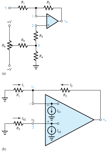
(a) Consider the input-offset voltage-nulling circuit for an inverting amplifier shown in Figure (a). Let R1 = 1.5k ,R2 = 22 k, R6 = 100 k, R5 = 500 k, R4 = 200 , and V = 12 V. Find the range of input offset voltages that can be generated at terminal 2 of the op amp. Also find R3 such that the input terminals see the same external resistance to ground.

(b) To examine the effects of input bias currents on the inverting amplifier, consider the circuit shown in Figure. Show that it is desirable to choose R3, which is equal to a parallel combination of R1 and R2. Compare the residual output voltage to what occurs if R3 were zero.

(c) Reconsider the circuit of part (b). Let R1 = 5k, and R2 = 70 k. Let the op-amp bias currents be Ib1 = 50 nA and Ib2 = 60 nA, but otherwise let the op amp be ideal. Determine the value of R3 that should be used.Also,when the input signal is zero, find the residual output offset voltage.

991_Find the residual output offset voltage.png


Related Discussions:- Find the residual output offset voltage

Determine the slip at maximum torque, A three-phase induction motor, operat...

A three-phase induction motor, operating at its rated voltage and frequency, develops a starting torque of 1.6 times the full-load torque and a maximum torque of 2 times the full-l

Design a multiplexer and anomalous signals, 1. The size of the multiplexer ...

1. The size of the multiplexer used to implement a truth table can be cut in half (e.g. 4 inputs instead of 8) if one of the variables is used as an input instead of being connecte

Find a minimum two level, Find a minimum two level, multiple-output AND-OR ...

Find a minimum two level, multiple-output AND-OR gate circuit to realize these functions (eight gates minimum). F 1 (a,b,c,d) =Σm(10,11,12,15) +D (4,8,14) F 2 (a,b,c,d) =Σm(4

Explain rs232c standard, Explain RS232C Standard. RS232C: 1. Stand...

Explain RS232C Standard. RS232C: 1. Standard described for asynchronous communications where there is given timing among data bits and no fixed timing among the characters

Human resources - kpi, Human Resources - KPI It is the responsibility ...

Human Resources - KPI It is the responsibility of management to have the lean, capable, customer friendly organization that strives for catering to diversified need of all the

Explain computer-aided circuit analysis, Q. Explain Computer-aided circuit ...

Q. Explain Computer-aided circuit analysis? A word of caution is appropriate if this is the student's first experience with simulation. Just as the proliferation of calculators

State thevenin'' s theorem, Thevenin' s Theorem Thevenins Theorem state...

Thevenin' s Theorem Thevenins Theorem states: "Any linear circuit containing several energy source and resistances can be replaced by just a Single Voltage in series with a

Explain the construction of depletion mosfet, Q. Explain the construction o...

Q. Explain the construction of depletion MOSFET? A slab of p-type material is formed from a silicon base and it is referred to as the substrate. It is the foundation upon which

What are transmission bridges, Q. What are transmission bridges? How do the...

Q. What are transmission bridges? How do they assist in satisfying the connectivity?  Ans: A typical transmission bridge is demonstrated in figure. Series capacitance and shunt

Write Your Message!

Captcha
Free Assignment Quote

Assured A++ Grade

Get guaranteed satisfaction & time on delivery in every assignment order you paid with us! We ensure premium quality solution document along with free turntin report!

All rights reserved! Copyrights ©2019-2020 ExpertsMind IT Educational Pvt Ltd