Find dispersion relation for free electron, Electrical Engineering

Assignment Help:

Find Dispersion Relation for Free Electron

Question: Find the dispersion relation for a free electron, and, thus, observe the relation between its rest mass and effective mass.

Solution: For a free electron, the electron momentum is  p =m0v = hk. Thus, E=m0V2/2=p2/ (2m0) = h2k2/(2m0). Therefore, the dispersion relation, i.e., E-k relation is parabolic. Hence, mx = h2/∂2Ε/∂K2=m0. This is a very interesting relation that says states that for a free electron, the rest mass and effective mass are one and similar, which is because of the parabolic band structure. Several materials have non-parabolic E-k relation, and, so they have quite different rest mass and effective mass for electrons.

Note: the effective mass may become a function of energy, for severely non-parabolic band structures, however, near the minima of the conduction band and towards the maxima of the valence band, the band structure can be taken to be parabolic, and, thus, an effective mass, which is independent of energy, may be obtained.

  • Thus, the effective mass is an inverse function of the curvature of the E-k diagram: weak curvature gives large mass, and strong curvature gives small mass.
  • Note that in general, the effective mass is a tensor quantity, however, for parabolic bands, it is a constant.
  • Another interesting feature is that the curvature d2E/dk2 is positive at the conduction band minima, however, it is negative at the valence band maxima.
  • Thus, the electrons near the top of the valence band have negative effective mass.
  • Valence band electrons with negative charge and negative mass move in an electric field in the same direction as holes with positive charge and positive mass.
  • Thus, the charge transport in the valence band can be fully accounted for by considering hole motion alone.
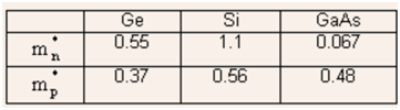
  • The electron and hole effective masses are denoted by m*n and m*p  respectively.


Table: the effective mass for electrons and holes (Χ m0, where m0 is the rest mass for electrons)311_Find Dispersion Relation for Free Electron.png


Related Discussions:- Find dispersion relation for free electron

Pn diode, PN Diode The current-voltage characteristics are of major ...

PN Diode The current-voltage characteristics are of major concern in the learning of semiconductor devices with light entering like a third variable in optoelectronics devic

Explain various functions of telephone switching systems, Q. Explain variou...

Q. Explain various functions of telephone switching systems. Ans: Functions of telephone switching systems are: (i)  Attending: The system should be continually monito

Drift current density and conductivity, Drift Current Density and Conductiv...

Drift Current Density and Conductivity: Consider a conductor of length / meters and cross sectional area a square meters, as shown in Fig. Let the number of free electrons ava

Tvm, Why is the signal first attenuated and then amplified?

Why is the signal first attenuated and then amplified?

Explain the configuration of a step-by-step switching system, With neat dia...

With neat diagrams explain the configuration of a step-by-step switching system. Schematic diagram for such an exchange is given in Figure.  Every subscriber is connected to a

ADC and DAC design, I''m trying to design ADC using MAX1198 and DAC using I...

I''m trying to design ADC using MAX1198 and DAC using IDAC in Multisim 12 but none of them are working. I need some help in this regard

What is rxd, What is RXD? RXD- Receive Data Input This input pin of ...

What is RXD? RXD- Receive Data Input This input pin of 8251A gets a composite stream of the data to be received by 8251A.

Draw the phasor diagrams for an rlc series circuit, Draw the phasor diagram...

Draw the phasor diagrams for an RLC series circuit supplied by a sinusoidal voltage source with a lagging power factor and a GLC parallel circuit supplied by a sinusoidal current s

Structure and use of pnp transistor, Structure and use of PNP transistor: ...

Structure and use of PNP transistor: The figure opposite is a schematic presentation of a PNP transistor related to two voltage sources. To construct the transistor conduct ap

Op, Find the current through capacitor by superposition therom

Find the current through capacitor by superposition therom

Write Your Message!

Captcha
Free Assignment Quote

Assured A++ Grade

Get guaranteed satisfaction & time on delivery in every assignment order you paid with us! We ensure premium quality solution document along with free turntin report!

All rights reserved! Copyrights ©2019-2020 ExpertsMind IT Educational Pvt Ltd