Explain balanced wye-connected load, Electrical Engineering

Assignment Help:

Balanced Wye-Connected Load

Let us consider a three-phase, four-wire 208-V supply system connected to a balanced wye connected load with an impedance of 10 20° , as shown in Figure (a). We shall solve for the line currents and draw the corresponding phasor diagram.

Conventionally it is assumed that 208 V is the rms value of the line-to-line voltage of the supply system, and the phase sequence is positive, or A-B-C, unless mentioned otherwise. The magnitude of the line-to-neutral (or phase) voltages is given by 208/√3, or 120 V. Selecting the line currents returning through the neutral conductor, as shown in Figure, we have

1407_Balanced Wye-Connected Load.png

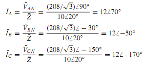
Note that ¯VBC has been chosen arbitrarily as the reference phasor, as in Figure (b). Assuming the direction of the neutral current toward the load as positive, we obtain

1532_Balanced Wye-Connected Load1.png

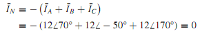
That is to say that the system neutral and the star point of the wye-connected load are at the same potential, even if they are not connected together electrically. It makes no difference whether they are interconnected or not.

Thus, for a balanced wye-connected load, the neutral current is always zero. The line currents and phase currents are equal inmagnitude, and the line currents are in phasewith the corresponding phase currents. The line-to-line voltages, in magnitude, are √3 times the phase voltages, and the phase voltages lag the corresponding line voltages by 30°.

The phasor diagram is drawn in Figure(b), from which it can be observed that the balanced line (or phase) currents lag the corresponding line-to-neutral voltages by the impedance

55_Balanced Wye-Connected Load2.png

angle (20° in our example). The load power factor is given by cos 20° for our problem, and it is said to be lagging in this case, as the impedance angle is positive and the phase current lags the corresponding phase voltage by that angle.

The problem can also be solved in a simpler way by making use of a single-line equivalent circuit, as shown in Figure(c),

303_Balanced Wye-Connected Load3.png

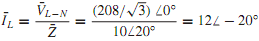
in which ¯ VL-N is chosen as the reference for convenience. The magnitude of the line current and the power factor angle are known; the negative sign associated with the angle indicates that the power factor is lagging. By knowing that the line (or phase) currents ¯IA, ¯IB, ¯IC lag their respective voltages ¯VAN, ¯VBN, and ¯VCN by 20°, the phase angles of various voltages and currents, if desired, can be obtained with respect to any chosen reference, such as ¯VBC.


Related Discussions:- Explain balanced wye-connected load

Emitter follwer, Ask questertion #Minimum 100 words accepted#

Ask questertion #Minimum 100 words accepted#

Show silicon n-channel jfet, Q. Given that a silicon n-channel JFET has V P...

Q. Given that a silicon n-channel JFET has V P = 5 V and I DSS = 12 mA, check whether the device is operating in the ohmic or active region when v GS =-3.2 V and i D = 0.5 mA.

Full wave rectifier with filter, what is the theory for full wave rectifier...

what is the theory for full wave rectifier with c filter

Machine, explain inifinite bus

explain inifinite bus

Electronics, The mobility of free electrons and holes for pure silicon are ...

The mobility of free electrons and holes for pure silicon are 0.13 and 0.05 m2/V-S respectively. Find the intrinsic conductivity for silicon. Assuming ni = 1.5x 10¹⁶/cm3 at room te

List out the five categories of the 8085 instructions, List out the five ca...

List out the five categories of the 8085 instructions. Give examples of the instructions for each group. 1.  Data transfer group - MOV, MVI, LXI. 2.  Arithmetic group - ADD,

Circuit symbols for mosfet, Circuit Symbols for MOSFET A range of symb...

Circuit Symbols for MOSFET A range of symbols are employed for the MOSFET. The basic design is usually a line for the channel along with the source and drain leaving it at rig

Binary coded decimal to decimal conversions, Binary Coded Decimal to Decima...

Binary Coded Decimal to Decimal Conversions • Step1. Break up the Binary Coded Decimal number into 4 bit binary number, starting from the least significant binary bit. • Step2

Find the diode current and voltage in given circuit, We shall demonstrate l...

We shall demonstrate load-line analysis to find the diode current and voltage, and then compute the total power output of the battery source in the circuit of Figure (a), given the

Write Your Message!

Captcha
Free Assignment Quote

Assured A++ Grade

Get guaranteed satisfaction & time on delivery in every assignment order you paid with us! We ensure premium quality solution document along with free turntin report!

All rights reserved! Copyrights ©2019-2020 ExpertsMind IT Educational Pvt Ltd