Explain amplitude-shift keying, Electrical Engineering

Assignment Help:

Q. Explain Amplitude-shift keying?

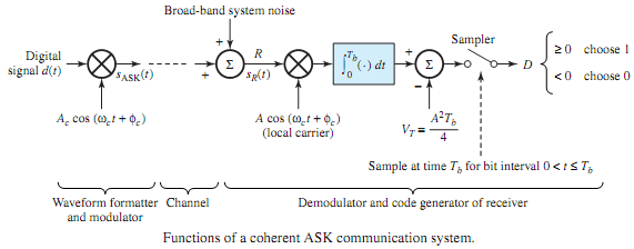
A carrier's amplitude is keyed between two levels (binary 1 and 0) in binary ASK. Figure shows the functions of a coherent ASK communication system. Let us consider a bit interval from 
1785_Explain Amplitude-shift keying.png


t = 0 to t = Tb, since the operation of any other interval will be similar. The desired ASK signal is given by

48_Explain Amplitude-shift keying1.png

where Ac, ωc, and φc are the peak amplitude, angular frequency, and phase angle of the modulated carrier, respectively. Equation can be viewed as a carrier Ac cos(ωct + φc) modulated by a digital signal d(t) that is 0 or 1 in a given bit interval. The digital signal and product device shown in Figure are then equivalent to the waveform formatter and modulator. Assuming that the received signal sR(t) differs only in amplitude from sASK(t), one can write

252_Explain Amplitude-shift keying2.png

The product device in the receiver's demodulator acts like a synchronous detector that removes the input carrier. The major disadvantage of the coherent ASK is that the required local carrier must be phase-connected with the input signal. The input to the integrator is a unipolar PCM signal, and the remainder of Figure is a PCM receiver.

The noncoherent ASK system eliminates the need for a coherent local oscillator. Figure shows the demodulator and code generator for a noncoherent ASK system. A matched filter (that has its impulse response matched to have the same form as the carrier pulse at its input) and envelope detector take the place of the synchronous detector and integrator of Figure.  While ASK systems are not as widely used as other systems for various reasons, the ASK concept remains significant, particularly as applied to modern optical communication systems which use intensity modulation of a light source.
154_Explain Amplitude-shift keying3.png


Related Discussions:- Explain amplitude-shift keying

What is memory paging, What is memory paging? The memory paging mechan...

What is memory paging? The memory paging mechanism located inside the 80386 and above permits any physical memory location to be assigned to some linear address.

What are hard magnetic materials, What are hard magnetic materials? Har...

What are hard magnetic materials? Hard Magnetic materials- They have a slowly rising magnetization curve along with large hysteresis loop area and therefore large energy losses

What are the various types of amplifiers, Q. What are the various types of ...

Q. What are the various types of amplifiers? Amplifiers can be classified as follows: (a) Based on the transistor configuration 1. Common emitter amplifier 2. Common c

Obtain an expression for the induced emf, Q. Consider a conducting loop of ...

Q. Consider a conducting loop of length l and width w, as shown in Figure, rotated about its axis (shown by the broken line) at a speed of ωm rad/s under the influence of a magneti

3 phase meter, What is reading mechanism of a 3 phase meter?

What is reading mechanism of a 3 phase meter?

Why do we cascade amplifiers, Q. Why do we cascade amplifiers? Why is RC co...

Q. Why do we cascade amplifiers? Why is RC coupling the most widely used coupling between 2 stages of a cascading amplifier? The voltage or power gain or frequency response obt

Switching characteristics, Switching Characteristics Switching  charact...

Switching Characteristics Switching  characteristics  of BJT  are shown  in figure. Due  to the presence of internal  capacitances BJT  cannot be  turned  instantly. Initially

Four cells in series, A battery having of 12 cells are divided in three gro...

A battery having of 12 cells are divided in three group which each group having of four cells in series. The three groups are joined in parallel. The emf of every cell is 1.5V and

What is the voltage gain of common gate amplifier, Q. What is the voltage g...

Q. What is the voltage gain of common gate amplifier? The controlled source gmVgs is connected from drain to source with rd in parallel.The resistor is connected Rs is connecte

What is extended data output ram, What is extended data output RAM? EDO...

What is extended data output RAM? EDO RAM: A slight modification to the DRAM structure changes the device in an EDO (extended data output) DRAM device. Inside the EDO memory, a

Write Your Message!

Captcha
Free Assignment Quote

Assured A++ Grade

Get guaranteed satisfaction & time on delivery in every assignment order you paid with us! We ensure premium quality solution document along with free turntin report!

All rights reserved! Copyrights ©2019-2020 ExpertsMind IT Educational Pvt Ltd