Energy bands, Electrical Engineering

Assignment Help:

Energy Bands

1) Since isolated atoms are brought together to make a solid, the electron wave functions begin to overlap.

2) Several interactions occur, and, at the proper interatomic spacing for the crystal, the forces of attraction and repulsion find a balance.

3)  Because of Pauli Exclusion Principle, the discrete energy levels of individual atoms split into bands relating to the pair instead of to individual atoms.

4)  In a solid, because of large number of atoms, the split energy levels for necessarily continuous bands of energy.

1247_Energy Bands.png

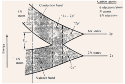
        Figure: Splitting  of  individual  energy  levels  to  energy  bands  as  atoms  are  brought  closer together.

5) Imaginary creation of a diamond crystal from isolated carbon atoms (1s22s22p2).

6) Every atom has two 1s states, two 2s states, six 2p states, and higher states.

7) For N atoms, the no.  of  states  are  2N,  2N,  and  6N  of  type  1s,  2s,  and  2p respectively.

8) Along with a reduction in the interatomic spacing, these types of energy levels split into bands, and the 2s and 2p bands merge into a single band comprising 8N available states.

9) Since the interatomic spacing arrives at the equilibrium spacing of diamond crystal, this band splits into two bands separated by an energy gap Eg, in which no allowed energy states for electrons exists => forbidden gap.

10) The upper band (termed as the conduction band) and the lower band (termed as the valence band) contain 4N states each.

11) The lower 1s band is filled along with 2N electrons, though the 4N electrons residing in the original n = 2 states will now inhabit states either in the valence band or in the conduction band.

12) At 0 K, the electrons will inhabit the lowest energy states available to them => so, the 4N  states  in  the  valence  band  will  be  totally  filled,  and  the  4N  states  in  the conduction band will be totally empty.


Related Discussions:- Energy bands

Pn diode, PN Diode The current-voltage characteristics are of major ...

PN Diode The current-voltage characteristics are of major concern in the learning of semiconductor devices with light entering like a third variable in optoelectronics devic

D.c.machines, can voltage regulation be negative?why?

can voltage regulation be negative?why?

Gis based mapping of electrical network, GIS Based Mapping of Electrical Ne...

GIS Based Mapping of Electrical Network: You have learnt in which the Geographic Information System is a system of mapping of the complete electrical network. The question we

New asic design flow, There is a requirement to propose a new ASIC design f...

There is a requirement to propose a new ASIC design flow within your company, from VHDL design capture through to GDSII tape out.  It is very important that the flow includes all t

Binary coded decimal addition, Q. Binary Coded Decimal Addition Now as ...

Q. Binary Coded Decimal Addition Now as in conventional decimal addition, Binary Coded Decimal addition is performed one decimal digit at a time. What happens when the sum g

Explain ramp type dvm, SOL. Ramp Type VM: The operating principle of the r...

SOL. Ramp Type VM: The operating principle of the ramp type DVM is based on the measurement of the time it takes for a linear ramp voltage to rise from 0 V to the level of the inp

Steps to develop microprocessor based computer system, Explain in brief ste...

Explain in brief steps to develop a Microprocessor based computer system. The design of a microcomputer system should begin with the CPU module. It modules establishes the fund

Gauss, research paper on gauss,s law?

research paper on gauss,s law?

Write Your Message!

Captcha
Free Assignment Quote

Assured A++ Grade

Get guaranteed satisfaction & time on delivery in every assignment order you paid with us! We ensure premium quality solution document along with free turntin report!

All rights reserved! Copyrights ©2019-2020 ExpertsMind IT Educational Pvt Ltd