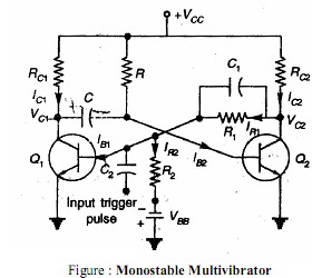
Q. Draw and explain a monostable multivibrator ?
The monostable configuration consists of two amplifier stages interconnected in such a manner as to possess one stable state. The circuit diagram of a monostable multi is shown in fig 1.The output of transistor A1 at y2 is coupled to the input at x1 through a resistor attenuator in which C1 is a small commutating capacitor. The dc coupling found in a binary from y1 to x2 is here replaced by capacitive coupling through C. While the resistor R at the input of A2 is shown returned to the supply voltage VCC, this feature of the circuit is not essential and R may be returned to a lower potential.
As you can see in the schematic diagram to the right, the monostable multivibrator is very similar in design to the bistable multivibrator you have already demonstrated. The primary difference is the use of a capacitor (C in the schematic) as one of the cross-coupling elements. The resistor is still present (R in the schematic), but now connects the base of Q2 to +5 volts instead of to the collector of Q1.
Of course, the capacitor will take a certain amount of time to charge, but once it does so it will carry no current, and Q2 will be turned on by the current through its 15K base resistor. This in turn holds the Q output at logic 0. This output is also applied as before, holding Q1 off. Assuming the T (Trigger) input is also quiescent at logic 0, Q3 is also off and the circuit will remain indefinitely in this state.
At this point, C is charged to just about +5 volts (less VBE of Q2), with the Q1 collector connection being positive. The circuit will remain in this state until a logic 1 signal is applied to the T input.
When an input signal is received at T, Q3 turns on and pulls the left end of capacitor C down to ground. Since the capacitor voltage cannot change instantaneously, this forces the right end of C to -5 volts, immediately turning Q2 off. This in turn applies a logic 1 to Q1's input, turning Q1 on. At this point, the input to T can be discontinued; the Q output is logic 1 and Q1 will remain on.
Under these circumstances, the left end of C remains locked to ground through Q1's collector. But the right end gradually charges through R, Q2's base resistor, towards +5 volts.
However, it never gets there; as soon as this voltage allows Q2's base to become forward biased, Q2 turns on and turns Q1 off again. This returns the circuit to its quiescent state. Thus, this circuit cannot maintain a logic 1 output indefinitely; this is not really a stable state for this circuit. The circuit has only one stable state (Q = 0). It is therefore known as a monostable multivibrator.