Direct and indirect semiconductors, Electrical Engineering

Assignment Help:

Direct and Indirect Semiconductors

1) In a common quantitative calculation of band structures, the wave function of a single electron traveling by a perfectly periodic lattice is assumed to be in the type of a plane wave moving in the x-direction (say) with propagation constant k, as well called a wave vector.

2) In quantum mechanics, the electron momentum can be provided by p= hk.

3) The wave function that is space dependent for the electron is ΨK (X) = U (Kx,x) ejK,x  in which the function U(Kx,x) modulates the wave function as per to the periodicity of the lattice.

4) Allowed values of energy, where as plotted as a function of k, gives the E-k diagram.

5) As the periodicity of most lattices is different in several directions, the E-k diagram is a complex surface that is to be visualized in three dimensions.

6) Direct band gap semiconductor: the minima of the conduction band and the maxima of the valence band take place at the same value of k => an electron creating the smallest energy transition from the conduction band to the valence band can do so with no a change in k (and, the momentum).

1968_Direct and Indirect Semiconductors.png

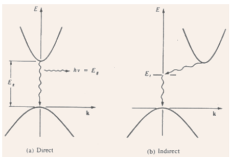
Figure:  Direct and indirect transition of electrons from the conduction band to the valence band:  (a) direct - with accompanying photon emission, (b) indirect via defect level.  

7) Indirect band gap semiconductor: the minima of the conduction band and the maxima of the valence band take place for different values of k, so, the smallest energy transition for an electron needs a change in momentum.

8) Electron  that falling  from  conduction  band  to  an  empty  state  in  valence  band => recombination.

9) Recombination possibility for direct band gap semiconductors is much higher than as compared to that for indirect band gap semiconductors.

10) Direct band gap semiconductors give up the energy released throughout this transition (=Eg) in the form of light => employed for optoelectronic applications (e.g., LEDs and LASERs).

11) Recombination in indirect band gap semiconductors takes place by some defect states within the band gap, and the energy is released in the type of heat given to the lattice.


Related Discussions:- Direct and indirect semiconductors

Determine kva rating of the auto - transformer, Q. A 15-kVA, 2200:220-V, tw...

Q. A 15-kVA, 2200:220-V, two-winding, single- phase transformer is connected as an autotrans- former to step up voltage from 220 V to 2420 V. Without exceeding the rated current of

What is voltage multiplying dacs, What is Voltage Multiplying DACs? Mul...

What is Voltage Multiplying DACs? Multiplying DACs function on the principle of producing a weighted sum analog signal where the sum is proportional to the digital input signal

Dc, what is quantization noise

what is quantization noise

Explain the suitability of aluminium, Explain the suitability of aluminium ...

Explain the suitability of aluminium  that is used as electrical conducting materials. Aluminium : Conductors are appropriate for ambient and very high temperature. Use of alu

What is session layer, Q. What is Session Layer? Session layer is used ...

Q. What is Session Layer? Session layer is used to allow users to identify themselves when waiting access to the network. This is concerned with setting up and sustaining an op

Program implementing the conjugate gradient method, Write a program impleme...

Write a program implementing the conjugate gradient method (un-preconditioned). Solve the  matrix equation corresponding to a finite difference node-spacing, h = 0.02m in x and y d

Give the principle of biasing a fet amplifier, Q. Give the principle of bia...

Q. Give the principle of biasing a FET amplifier. To correctly bias the FET, the gate needs to be negative with respect to the source. Bias is obtained in the following manner:

Explain how leds are arranged in a seven segment display, Q. Explain how LE...

Q. Explain how LEDs are arranged in a seven segment display ? The illustration given below shows the basic layout of the segments in a seven- segment display. The segments the

Rectification, diagram for full wave bridge circuit single phase,full wave ...

diagram for full wave bridge circuit single phase,full wave centre tap circuit and haif wave rectification circuit

Design a circuit using real components, The circuit shown below is a protot...

The circuit shown below is a prototype 4 th - order low-pass filter which is required to meet the specification given. However the specification is not met due to inadequate atten

Write Your Message!

Captcha
Free Assignment Quote

Assured A++ Grade

Get guaranteed satisfaction & time on delivery in every assignment order you paid with us! We ensure premium quality solution document along with free turntin report!

All rights reserved! Copyrights ©2019-2020 ExpertsMind IT Educational Pvt Ltd