Diode transistor logic gate, Electrical Engineering

Assignment Help:

A circuit realization of a NAND gate will now be developed. By connecting NAND gates together in various ways, one can synthesize other gates and flip-flops. Thus in principle, a single NAND gate circuit, repeated many times, would be sufficient to build up digital systems. One possible NAND gate circuit is shown in Figure, in which it can have asmany inputs as desired (indicated by the dashed-line input C), and typical values of VCC = 5V, RA = 2k, RC = 5k, and β = 50. We shall now consider the two inputs A and B that are quite adequate for our discussion,with the high range defined to be 4 to 5Vand the lowrange defined to be 0 to 0.5V.

555_Diode Transistor Logic Gate.png

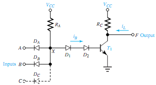
While the input voltages vA and vB are constrained to lie inside the high or low range of the allowed voltage ranges, the resulting output voltage vF is supposed to be inside the high or low range as well. For different combinations of vA and vB, we need to find vF. Since the circuit consists of no less than five nonlinear circuit elements (DA, DB, D1, D2, and T1), an approximation technique is used for analysis, while taking the voltage across a current-carrying forward-biased pn junction to be 0.7 V. The reader may have realized that it is not obvious at the start which diodes are forward-biased and which are reverse-biased. Hence a guessing procedure is used in which a guess is made and checked for self-consistency.

Let us start by letting vA = vB = 0, in which case a probable current path is from VCC down through RA and through inputs A and B. Since this guess implies current flow through DA and DB in the forward direction, wemay guess that the voltage at X is 0.7 V. There is also a current path from X down to ground through D1 and D2 and the base-emitter junction of the transistor. Even though the sign of the guessed voltage is correct to forward-bias these three junctions, its magnitude of 0.7 V is insufficient since 2.1 V (or 3 × 0.7) is needed to make current flow through this path.


Related Discussions:- Diode transistor logic gate

States ohm''s law, States Ohm's law Ohm's law describes that the curren...

States Ohm's law Ohm's law describes that the current I flowing in a circuit is directly proportional to the applied voltage V and inversely proportional to the resistance R, g

Fast recovery diodes - types of power diodes , Fast  Recovery diodes ...

Fast  Recovery diodes The fast  recovery  diodes low recovery times. These diodes  are manufactured by diffusion. They are used in converter circuits where  the speed  of reco

Find the average power absorbed by each element, Q. Let v(t) = V max cos ω...

Q. Let v(t) = V max cos ωt be applied to (a) a pure resistor, (b) a pure capacitor (with zero initial capacitor voltage, and (c) a pure inductor (with zero initial inductor curren

Explain factors affecting permeability and hysterisis loss, Explain the fac...

Explain the factors affecting permeability and hysterisis loss. Factors affecting permeability and hysterisis loss: When the initial permeability is high, the hysterisis los

Depletion type mosfet, Depletion type MOSFET The channel is of silico...

Depletion type MOSFET The channel is of silicon. It can be two type of channel that is an n-type or p-type channel; it is still mostly silicon. After that, we take note that

Electric Drive, project to write a program to simulate a dc motor on a matl...

project to write a program to simulate a dc motor on a matlab

Mechanism of metal removal in electrochemical machining, What is the proces...

What is the process of metal removal in electrochemical machining? What are the basic functions of electrolyte in ECM? Illustrate the following key terms in electrochemical mach

Sketch the phasor diagram of the voltage, Q. The line-to-line voltage of a ...

Q. The line-to-line voltage of a balanced wye connected three-phase source is given as 100 V. Choose V AB as the reference. (a) For the phase sequence A-B-C, sketch the phasor

Electric Optic Device, Transmission Through a LiNb0 3 Plate Examine the tr...

Transmission Through a LiNb0 3 Plate Examine the transmission of an unpolarized He-Ne laser beam (?o= 633 nm) normally incident on a LiNb0 3 plate (ne = 2.29, no = 2.20) of thickn

Write Your Message!

Captcha
Free Assignment Quote

Assured A++ Grade

Get guaranteed satisfaction & time on delivery in every assignment order you paid with us! We ensure premium quality solution document along with free turntin report!

All rights reserved! Copyrights ©2019-2020 ExpertsMind IT Educational Pvt Ltd