Diode Schematic Symbol
The diode in figure is a unidirectional device. Electron current just only flows in one direction, against the arrow, corresponding to forward bias. The cathode, bar, of the diode symbol corresponds to N-type semiconductor. The anode, arrow, corresponds to the P-type semiconductor. To memorize this relationship, Not-pointing (bar) on the symbol corresponds to N-type semiconductor. Pointing (arrow) corresponds to P-type.
If a diode is forward biased like in Figure above (a), current will get increase slightly as voltage is increased from 0 V. In the case of a silicon diode a computable current flows while the voltage approaches 0.6 V at (c). As greater the voltage is increases past 0.6 V, current increases significantly after the knee. Raising the voltage well beyond 0.7 V may result in high enough current to destroy the diode. The forward voltage, VF, is a characteristic of the semiconductor: 0.6 to 0.7 V for silicon, 0.2 V for germanium, some volts for Light Emitting Diodes (LED). The forward current ranges from a few mA for point contact diodes to 100 mA for small signal diodes to tens or thousands of amperes for power diodes.
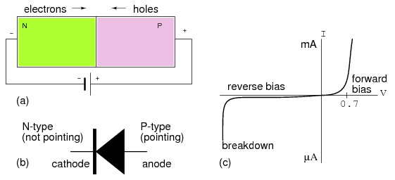
Figure: (a) Forward biased PN junction, (b) Corresponding diode schematic symbol (c) Silicon Diode I vs V characteristic curve.
Just only the leakage current of the intrinsic semiconductor flows, if the diode is reverse biased. This is planned to the left of the origin in diagram above(c). This current will just only be as high as 1 µA for the most intense conditions for silicon small signal diodes. This current does not increase noticeably with increasing reverse bias until the diode breaks down. At breakdown, the current get increases so significantly that the diode will be destroyed unless a high series resistance limits current. We generally select a diode with a higher reverse voltage rating than as compared to any applied voltage to prevent this. Silicon diodes are commonly available with reverse break down ratings of 50, 100, 200, 400, 800 V and higher. It is probable to fabricate diodes with a lower rating of a few volts for utilize as voltage standards.
We earlier mentioned that the reverse leakage current of within a µA for silicon diodes was because of conduction of the intrinsic semiconductor. This is the leakage which can be described by theory. Thermal energy generates few electron hole pairs that conduct leakage current until recombination. In concrete practice this predictable current is only part of the leakage current. Much of the leakage current is because of surface conduction, related to the lack of cleanliness of the semiconductor surface. Both of the leakage currents increase with growing temperature, approaching a µA for small silicon diodes.
Since the p-type material is now associated to the negative terminal of the power supply, 'holes' within the P-type material are pulled away from the junction, causing the width of the depletion zone to increase. Likewise, because the N-type region is linked to the positive terminal, the electrons will as well be pulled away from the junction. Hence the depletion region widens, and does so much increasingly with increasing reverse-bias voltage. This get increases the voltage barrier causing a high resistance to the flow of charge carriers thus permitting minimal electric current to cross the p-n junction. The increase in resistance of the p-n junction results in the junction to behave like an insulator. This is significant for radiation detection since if current was able to flow; the charged particles would just dissipate into the material. The reverse bias makes sure that charged particles are capable to create it to the detector system.