Difference between static and dynamic RAM. Draw the circuits of one cell of each and explain its working.
Ans:
Differentiation among Static RAM and Dynamic RAM:
Static RAMs store firstly and zeros by using conventional FLIP-FLOPs. While, the memory cells of dynamic RAMs are fundamentally charge storage capacitors along with driver transistors. The absence or presence of charge into a capacitor is interpreted as Logic 0 or 1.
Static RAMs do not need refreshing since there is no problem of charge leaking-off in FLIP-FLOPs while Dynamic RAMs need periodic charge refreshing to keep data storage since the charge stored on capacitors leak-off along with time.
Static RAMs are slower but simple to drive than dynamic memories, that generally need clock signals in addition to more power supplies while dynamic circuits usually need externally generated clock voltages,
Advantages of Static RAMs over Dynamic RAMs:
(i) Faster speed of operation (higher) that is lower access -time
(ii) Does not need refreshing.
Advantages of Static RAMs over Dynamic RAMs:
(i) Higher number of bits storage on a specified silicon chip area. That is Higher packaging density.
(ii) Consumption of lower power.
Static RAM Cell: A RAM memory cell having two cross-coupled MOS inverters is demonstrated in Fig. (a). This is addressed through setting AX and AY to 1. While AX = 1, the cell is links to the data and data‾ line. While AY = 1, T7 and T8 are ON.
To write the cell, set W = 1, T9 will be ON. If data input is 1, the voltage at node D will consequent to level 1 making T3 ON and level at D‾ will be 0. Conversely, if the data input is at logic 0, then T3 will be OFF and D‾ would be at 1. To understand writing or read the state of the FLIP-FLOP, firstly we set R = 1. It connects the data output to D‾. Therefore, the complement of the data‾ level written in the cell is read at data output.
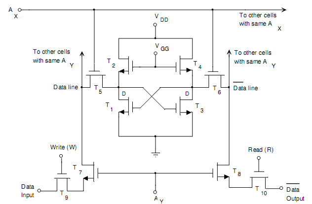
Fig.(a) Logic Diagram of a Static MOS RAM Cell
Dynamic RAM Cell: It uses four transistors in place of the six utilized in a static cell. It reduces the silicon chip area and outputs in saving of power. The circuit of a four-transistor dynamic MOS RAM cell is demonstrated in Fig.(b). The state of this cell is stored upon the stray capacitances C1 and C2, whose presence is necessary. The cell is addressed through making AX = AY =1. In individual state of the cell, the voltage across C1 is large and T1 is ON. Respectively, C2 has zero voltage and T2 is OFF. In another state, the voltages on C1 and C2 as well as the conducting states of T1 and T2 are reversed. To writing in the cell, we set W = 1 and also for reading from the cell we set R = 1. This is essential to refresh the cell periodically, or else the charge stored upon the capacitors leak off. Hence the refreshing operation is accomplished through permitting brief access from the provide voltage VDD to the cell. It is done through making AX = 1 furthermore the refresh terminal voltage consequent to 1 level. It makes T3, T4, T9, and T10 ON. Assume initially T1 is ON, T2 is OFF. So, the voltage across C1 is large and across C2 this is zero volts. Throughout the refresh interval, VDD is applied by T10 and T4 to C1, since T2 is OFF. Thus, current from VDD will flow through C1, permitting C1 to replenish any charge lost because of leakage. Since T1 is ON, thus C2 will not charge as quickly as C1. Likewise VDD is applied to C2, that is in parallel to T1 while T1 is OFF and T2 is ON.
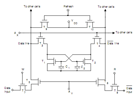
Fig.(b) Logic Diagram of Dynamic MOS RAM Cell