Development tools environment , Computer Engineering

Assignment Help:

Main Objectives:
• MPLAB In-Circuit Debugger (ICD 2) functionality
• ICD 2 Connection design
• MPLAB ICD 2 setup with the PC and Interface board designed
• I²C Protocol buses technologies

MPLAB In-Circuit Debugger (ICD 2)

The MPLAB ICD 2 debugger/programmer tool: is a low cost real-time debugger and programmer for selected PIC microcontrollers and dsPIC DSCs. The ICD 2 uses two dedicated hardware lines (PGC and PGD) or pins that control In Circuit Serial ProgrammingTM (ICSPTM) of the device and, afterwards, debugging through proprietary, on-chip firmware.
The features of ICD 2 debug are built into the microcontroller and activated by downloading the debug code into the target processor. Some shared overhead expenses are one stack level, general purpose file registers and a small area of program memory when in the debug mode.
The ICD 2 main functions are downloading programs into the microcontroller. The programs are executed in real time and examined in detail with the debug functions of MPLAB. Also set watch variables and breakpoints from symbolic labels in C or assembly source code, and single step through C source lines or into assembly code. MPLAB ICD 2 can also be used as a development programmer for supported MCUs.

ICD2 CONNECTOR

Main Objectives:

  1. To enable between the ICD2 connector and any suitable peripherals e.g. ICD2 Debugger
  2. Uploading data or codes into the PIC via the connector

This is a way of plugging a PIC into a standard computer (PC). A separate piece of hardware, called a "Programmer or ICD2 Debugger" is required to connect to one side of the PC I/O port to the PIC on the other side. There are other frequently used connectors such as the parallel port, serial port (COM port), the USB etc.

ICD2 CONNECTOR PIN OUT

Defining the pins of the connectors on an ICD2 cable as shown in Figure below:
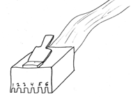
                        1654_ICD2.png

                                FIGURE: ICD2 cable

The standard In- Circuit Debugger (ICD2) cable is wired so that the pins are flipped between the ends. In other words, pin 1 on one end is connected to pin 6 on the other end, pin 2 to pin 5, etc. The pin out of each end is shown in table 3 below:
Table : ICD 2 PIN OUTS

Signal

ICD2 end pin    

Target end pin

VPP/ MCLR


6

    1

VDD

5

    2

GND

4

    3

PGD

3

    4

PGC

2

    5

not connected

1

    6


Related Discussions:- Development tools environment

Salient points about addressing mode, Salient points about addressing mode ...

Salient points about addressing mode are:  This addressing mode is employed to initialise value of a variable. Benefit of this mode is that no extra memory accesses are

Addressing mode, the 68000 has rich of addressing mode . it concerned with ...

the 68000 has rich of addressing mode . it concerned with the way data is accessed . identify the destion addressing mode for EXG D0, A2

Micro processor code, Suppose that the working register W contains the valu...

Suppose that the working register W contains the value 0x4F, the register FSR contains the value 0x2B; the register with address 0x2B contains 0x2F and the instruction ADDWF INDF,

Meaning of every field in mips instruction, Q. Meaning of every field in MI...

Q. Meaning of every field in MIPS instruction? The meaning of every field in MIPS instruction is given below: op: operation code or opcode rs: First register source

Operation codes used in assembly instructions, Q. Operation codes used in a...

Q. Operation codes used in assembly instructions? Now let's describe various operation codes needed for this machine so that we can translate High level language instructions t

Is the address bus unidirectional, The address bus is unidirectional due to...

The address bus is unidirectional due to the address information is always given by the Micro Processor to address a memory location of an input or output devices.

How many ram chips are required for memory of 2048 bytes, How many 128 × 8 ...

How many 128 × 8 RAM chips are required to provide a memory capacity of 2048 bytes. Ans. Available here RAM chips = 128 x 8 Required the memory capacity    = 2048 x 8 No. of chip

What are the layers of data description in r/3, What are the layers of data...

What are the layers of data description in R/3? There layesr are there:- The external layer. The ABAP/4 layer. The database layer.

Use of instruction register and program counter, Use of instruction registe...

Use of instruction register and program counter: Q. What is the use of instruction register (IR) and program counter (PC)? Ans: The instruction register (IR) holds the inst

Convert binary number in two''s compliment form, Convert binary number in t...

Convert binary number in two's compliment form 0100 1000. Converting the binary number into 2's compliment from 0100 1000 is given below: 01001000 => 10111000

Write Your Message!

Captcha
Free Assignment Quote

Assured A++ Grade

Get guaranteed satisfaction & time on delivery in every assignment order you paid with us! We ensure premium quality solution document along with free turntin report!

All rights reserved! Copyrights ©2019-2020 ExpertsMind IT Educational Pvt Ltd