Data Validation condition: The following condition stated below must be met for a data to be valid as is shown in the figure 3a below.
1. The data on the SDA line must remain stable during the HIGH period of the clock.
2. The HIGH or LOW state of the data line can only change when the clock signal on the SCL line is LOW
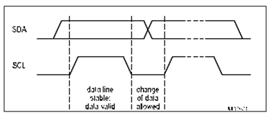
FIGURE: Data Validation condition
START AND STOP CONDITIONS
Some unique situations arise within the procedure of the I2C-bus, which are defined as START (S) and STOP (P) conditions as shown is figure 3b below. These conditions are always generated by the master. The bus is known to be busy state after the START condition. The bus is considered to be free again a certain time after the STOP condition
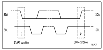
FIGURE : Start and Stop Conditions
Starts Condition - it occurs during a Low to High transition on the SDA line while SCL is remains high.
The microcontroller's samples the SDA line at least twice per clock period to sense the transition to detect the START and STOP conditions, but it very easy if the bus is incorporate the necessary interfacing hardware.
The bus remains busy if a repeated START (Sr) is generated instead of a STOP condition. Hence, the START (S) and repeated START (Sr) conditions are functionally identical. So the S symbol is used as a generic term to represent both the START and repeated START conditions, unless Sr is particularly relevant.
TRANSFERRING DATA
Data is transferred using byte format with the most significant bit (MSB) first. All byte put on the SDA line must be 8-bits long and there is no limit to the number of bytes that can be transmitted.
Each byte is to be followed by an acknowledge bit. If a slave can't receive or transmit another complete byte of data until it has performed some other function, for example running an internal interrupt, it can hold the serial clock line SCL low to force the master into a wait state.
The Data transfer continues when the slave is ready for another byte of data and releases clock line SCL. In some cases, it's allowed to use a different format from the I2C-bus format, for example (CBUS compatible devices). A message starting with such an address can be terminated by generation of a STOP condition, even during the transmission of a byte. In this case, no acknowledge is generated. How the data is transferred is shown in figure 3c below:
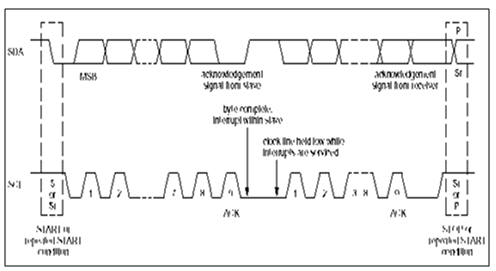
FIGURE : Start and Stop Conditions
DATA ACKNOWLEDGEMENT
It is compulsory to transfer data with acknowledge. The acknowledge-related clock pulse is produced by the master devices. The transmitter releases the SDA line (HIGH) during the acknowledge clock pulse. The receiver must pull down the SDA line during the acknowledge clock pulse in order to stays LOW during the HIGH period of this clock pulse putting set-up and hold times into account.
In general, an addressed receiver is obliged to generate an acknowledgement after each byte has been received. The master can now either generate a STOP condition to terminate the transfer, or a repeated START condition to establish a new transfer.
After the slave address is acknowledged by slave-receiver, and some time later in the transfer cannot receive any more data bytes, the master must again terminate the transfer.
This is indicated by the slave generating the not-acknowledge on the first byte to follow. The slave leaves the data line HIGH and the master generates a STOP or a repeated START condition. Whenever a master-receiver is involved in a transfer, it must signal the end of data to the slave- transmitter in order not to generate an acknowledgement on the last byte that was clocked out of the slave. The slave-transmitter must release the data line to allow the master to generate a STOP or repeated START condition.